Semiconductor device and method for manufacturing semiconductor device
- Summary
- Abstract
- Description
- Claims
- Application Information
AI Technical Summary
Benefits of technology
Problems solved by technology
Method used
Image

Examples
embodiment 1
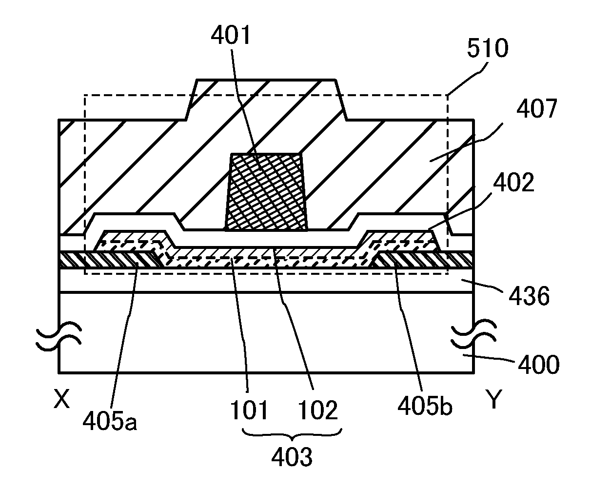
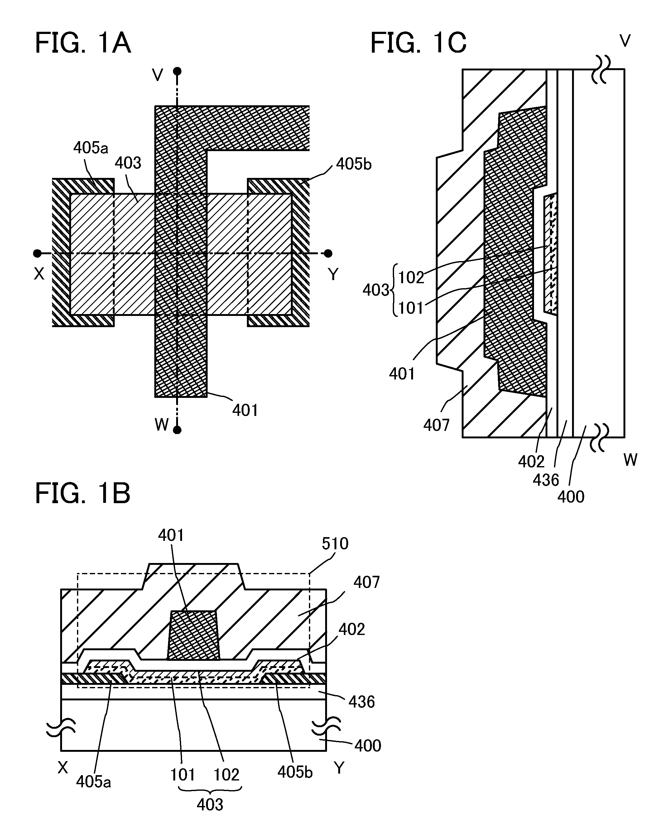
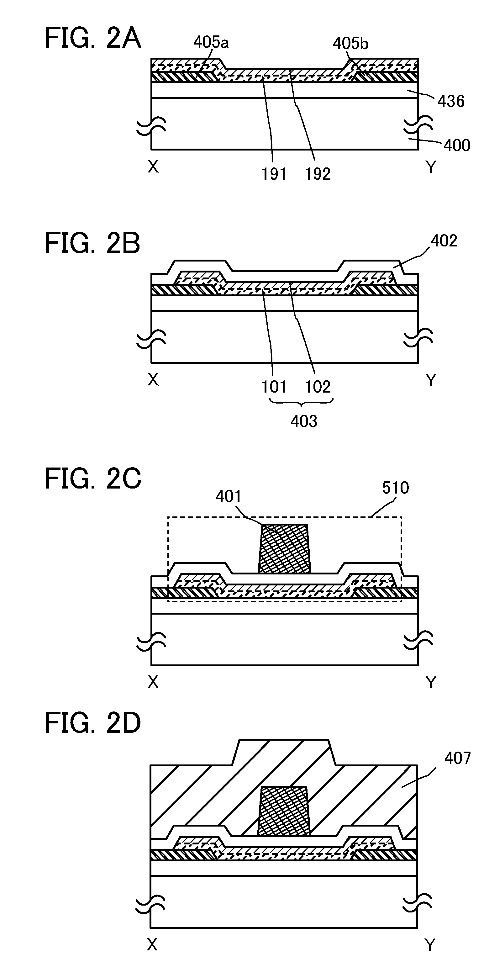
[0057]In this embodiment, one embodiment of a semiconductor device and one embodiment of a method for manufacturing the semiconductor device are described with reference to FIGS. 1A to 1C and FIGS. 2A to 2D. In this embodiment, a transistor including an oxide semiconductor stack is described as an example of the semiconductor device.
[0058]A transistor 510 illustrated in FIGS. 1A to 1C is an example of a top-gate transistor. FIG. 1A is a plan view, FIG. 1B is a cross-sectional view taken along chain line X-Y in FIG. 1A, and FIG. 1C is a cross-sectional view taken along chain line V-W in FIG. 1A.
[0059]As illustrated in FIG. 1B, which is a cross-sectional view in the channel length direction, the transistor 510 includes, over a substrate 400 which has an insulating surface and is provided with an oxide insulating film 436, a source electrode layer 405a, a drain electrode layer 405b, an oxide semiconductor stack 403 which is provided over the source electrode layer 405a and the drain el...
embodiment 2
[0128]In this embodiment, examples of a transistor which can be obtained by a process partly changed from that in Embodiment 1 are described with reference to FIGS. 3A to 3D, FIGS. 4A to 4D, and FIGS. 5A and 5B. In this embodiment, as for the same portions as Embodiment 1 or portions having functions similar to those in Embodiment 1 and steps, Embodiment 1 can be referred to and repetitive description is omitted.
[0129]A transistor 520 illustrated in FIGS. 3A to 3C is an example of a top-gate transistor. FIG. 3A is a plan view, FIG. 3B is a cross-sectional view taken along chain line X-Y in FIG. 3A, and FIG. 3C is a cross-sectional view taken along chain line V-W in FIG. 3A.
[0130]As illustrated in FIG. 3B, which is a cross-sectional view in the channel length direction, the transistor 520 includes, over the substrate 400 which has an insulating surface and is provided with the oxide insulating film 436, the source electrode layer 405a, the drain electrode layer 405b, the oxide semico...
embodiment 3
[0187]A semiconductor device having a display function (also referred to as a display device) can be manufactured using the transistor described in Embodiment 1 or 2. Moreover, some or all of driver circuits which include the transistor can be formed over a substrate where a pixel portion is formed, whereby a system-on-panel can be obtained.
[0188]In FIG. 6A, a sealant 4005 is provided to surround a pixel portion 4002 provided over a first substrate 4001, and the pixel portion 4002 is sealed using a second substrate 4006. In FIG. 6A, a scan line driver circuit 4004 and a signal line driver circuit 4003 each of which is formed using a single crystal semiconductor film or a polycrystalline semiconductor film over a substrate separately prepared are mounted in regions that are different from the region surrounded by the sealant 4005 over the first substrate 4001. Various signals and potentials are supplied to the pixel portion 4002 through the signal line driver circuit 4003 and the sca...
PUM
 Abstract
Description
Claims
Application Information
 - R&D
- Intellectual Property
- Life Sciences
- Materials
- Tech Scout
- Unparalleled Data Quality
- Higher Quality Content
- 60% Fewer Hallucinations
Browse by: Latest US Patents, China's latest patents, Technical Efficacy Thesaurus, Application Domain, Technology Topic, Popular Technical Reports.
© 2025 PatSnap. All rights reserved.Legal|Privacy policy|Modern Slavery Act Transparency Statement|Sitemap|About US| Contact US: help@patsnap.com