Method for Manufacturing Full Silicide Metal Gate Bulk Silicon Multi-Gate Fin Field Effect Transistors

a technology of metal gate bulk silicon and field effect transistor, which is applied in the field of semiconductors, can solve the problems of high manufacturing cost, reduced feature size of cmos devices, and severe challenge to the planar bulk silicon device with cmos, and achieves low gate sheet resistance, easy integration, and reduced manufacturing cost

Inactive Publication Date: 2013-01-10
INST OF MICROELECTRONICS CHINESE ACAD OF SCI
View PDF6 Cites 14 Cited by
  • Summary
  • Abstract
  • Description
  • Claims
  • Application Information

AI Technical Summary

Benefits of technology

[0024]1. A method for manufacturing a full silicide metal gate bulk silicon multi-gate fin field effect transistor is provided in the present invention, by which a fin field effect transistor device may be manufactured on the bulk silicon substrate, thus the self-heating effect and the floating body effect in the SOI FinFET device are overcome and the manufacturing cost is reduced;
[0025]2. A method for manufacturing a full silicide metal gate bulk silicon multi-gate fin field effect transistor is provided in the present invention, by which the

Problems solved by technology

With continuous development of the Integrated Circuitry (IC) industry under Moore' law, the feature size of CMOS device is continuously reduced, and the planar bulk silicon device

Method used


Image

  • Method for Manufacturing Full Silicide Metal Gate Bulk Silicon Multi-Gate Fin Field Effect Transistors
  • Method for Manufacturing Full Silicide Metal Gate Bulk Silicon Multi-Gate Fin Field Effect Transistors
  • Method for Manufacturing Full Silicide Metal Gate Bulk Silicon Multi-Gate Fin Field Effect Transistors

Examples


Embodiment Construction

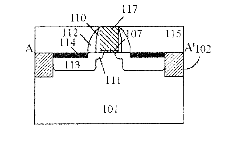
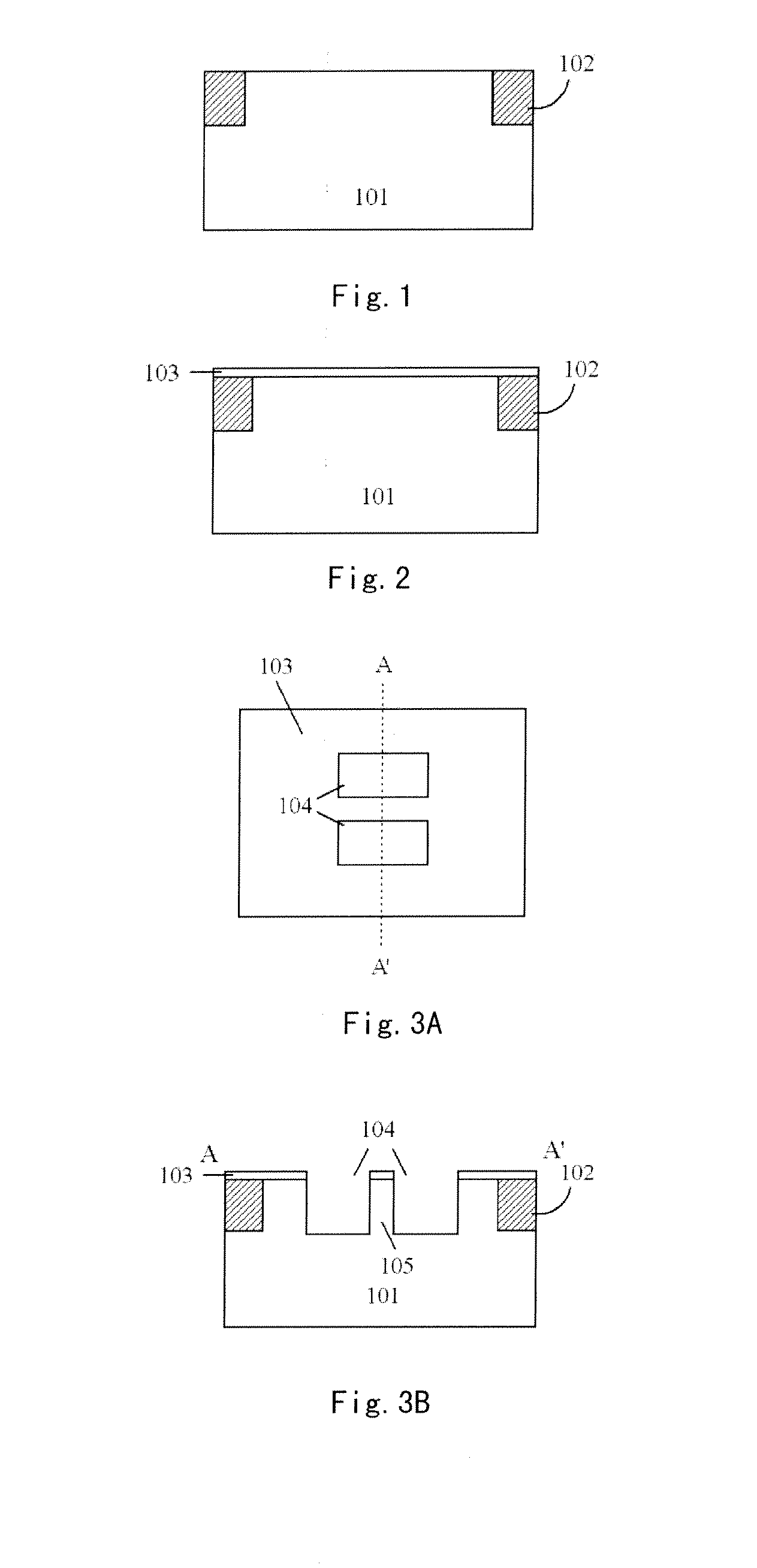
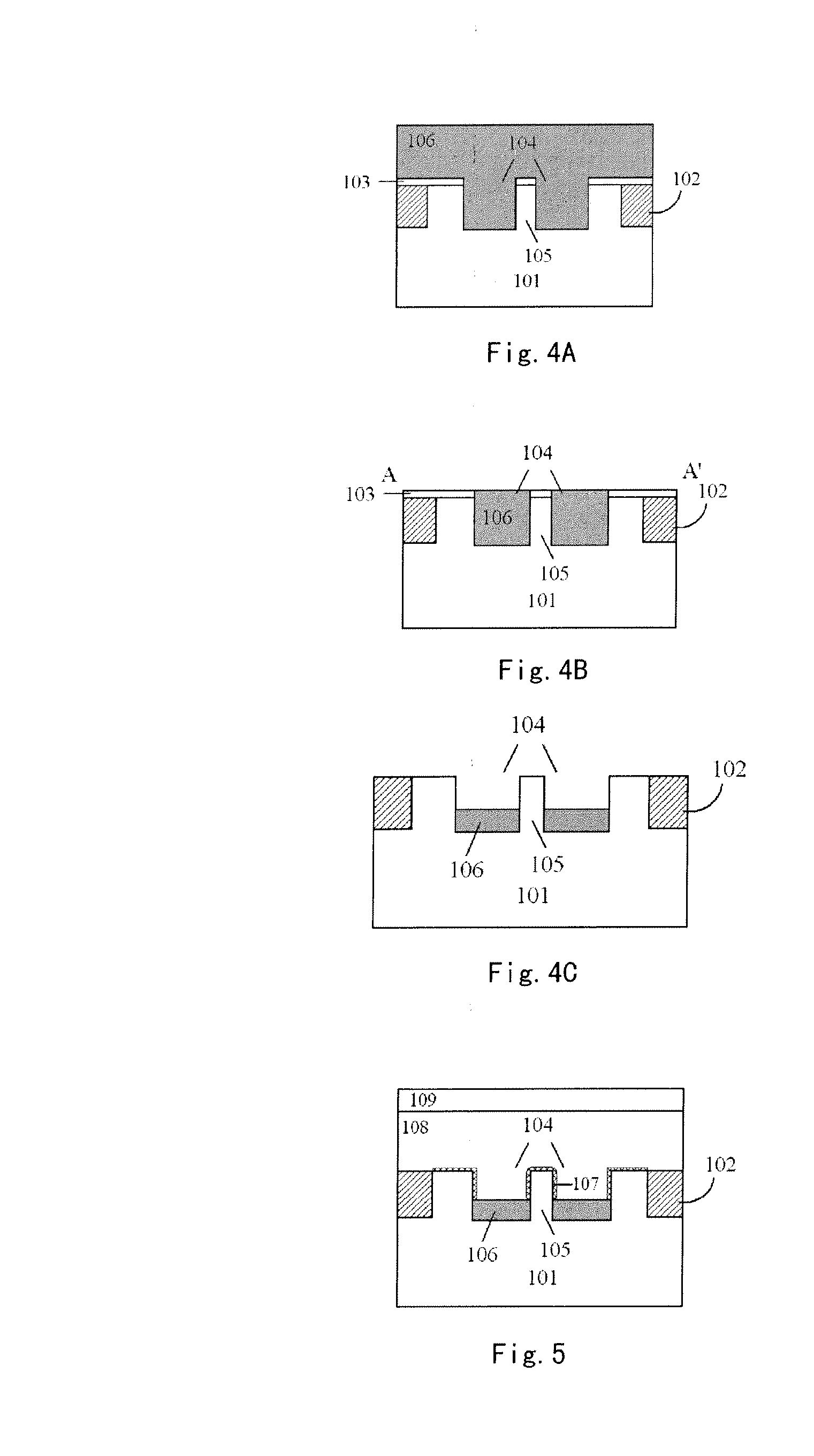
[0030]The present invention is described by the embodiments as illustrated in the drawings below. It should be appreciated that these descriptions are merely schematic, and do not intend to limit the scope of the invention. Furthermore, descriptions of common structures and techniques are omitted in the following description, avoiding unnecessary confusion of the concepts in the present invention.

[0031]Schematic diagrams showing layer structures according to the embodiments of the present invention are provided in the drawings. However, these diagrams are not drawn to scale, where some details may be magnified and some details may be omitted for clearness. The areas, and shapes of layers as well as relative size and positional relationships therebetween in the drawings are merely illustrative, and derivations may exist due to manufacturing tolerance or technical limitation in practice, besides areas / layers having different shapes, sizes and relative positions may be additionally des...


PUM


Abstract

The present application discloses a method for manufacturing a full silicide metal gate bulk silicon multi-gate fin field effect transistor, which comprises the steps of: forming at least one fin on the semiconductor substrate; forming a gate stack structure on top and side surfaces of the fin; forming a source/drain extension area in the fin on both sides of the gate stack structure; forming a source/drain area on both sides of the source/drain extension area; forming silicide on the source/drain area; forming a full silicide metal gate electrode; and forming contact and implementing metalization. The present invention eliminates the self-heating effect and the floating body effect of SOI devices, then has a much lower cost, overcomes such defects as the polysilicon gate depletion effect, Boron penetration effect, and large series resistance of polysilicon gate electrodes, and has good compatibility with the planar COMS technology, thus it can be easily integrated.

Description

FIELD OF THE INVENTION[0001]The present invention belongs to the semiconductor technical field, and particularly relates to a method for manufacturing a full silicide metal gate bulk silicon multi-gate fin field effect transistor.BACKGROUND OF THE INVENTION[0002]With continuous development of the Integrated Circuitry (IC) industry under Moore' law, the feature size of CMOS device is continuously reduced, and the planar bulk silicon device with CMOS is severely challenged. To overcome such problems, solutions may be found from many aspects such as new materials, new processes, and new structures.[0003]In the field of new materials, the technology of metal gate electrode is very important. The polysilicon gate depletion effect and Boron (B) penetration effect of a P-type field effect transistor may be thoroughly eliminated and meanwhile a very low gate sheet resistance may be acquired by using metal gate electrodes. Among various methods for manufacturing metal gates, the technology o...

Claims


Application Information

Patent Timeline
IPC IPC(8): H01L21/336
CPCH01L29/4975H01L29/66795
Inventor ZHOU, HUAJIEXU, QIUXIA
Owner INST OF MICROELECTRONICS CHINESE ACAD OF SCI
Why Eureka
Try Eureka