Plasma processing method and plasma ashing apparatus
a plasma ashing and processing method technology, applied in the direction of cleaning processes and apparatus, chemistry apparatus and processes, electric discharge tubes, etc., can solve the problems of reducing the mechanical strength, increasing the relative dielectric constant of the low-k film, and reducing the film thickness, so as to prevent or reduce the damage of the film. , the effect of high-speed ashing processing
- Summary
- Abstract
- Description
- Claims
- Application Information
AI Technical Summary
Benefits of technology
Problems solved by technology
Method used
Image
Examples
first embodiment
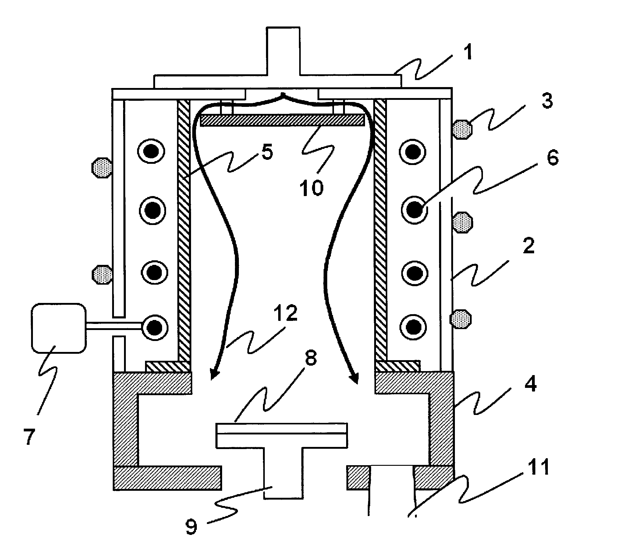
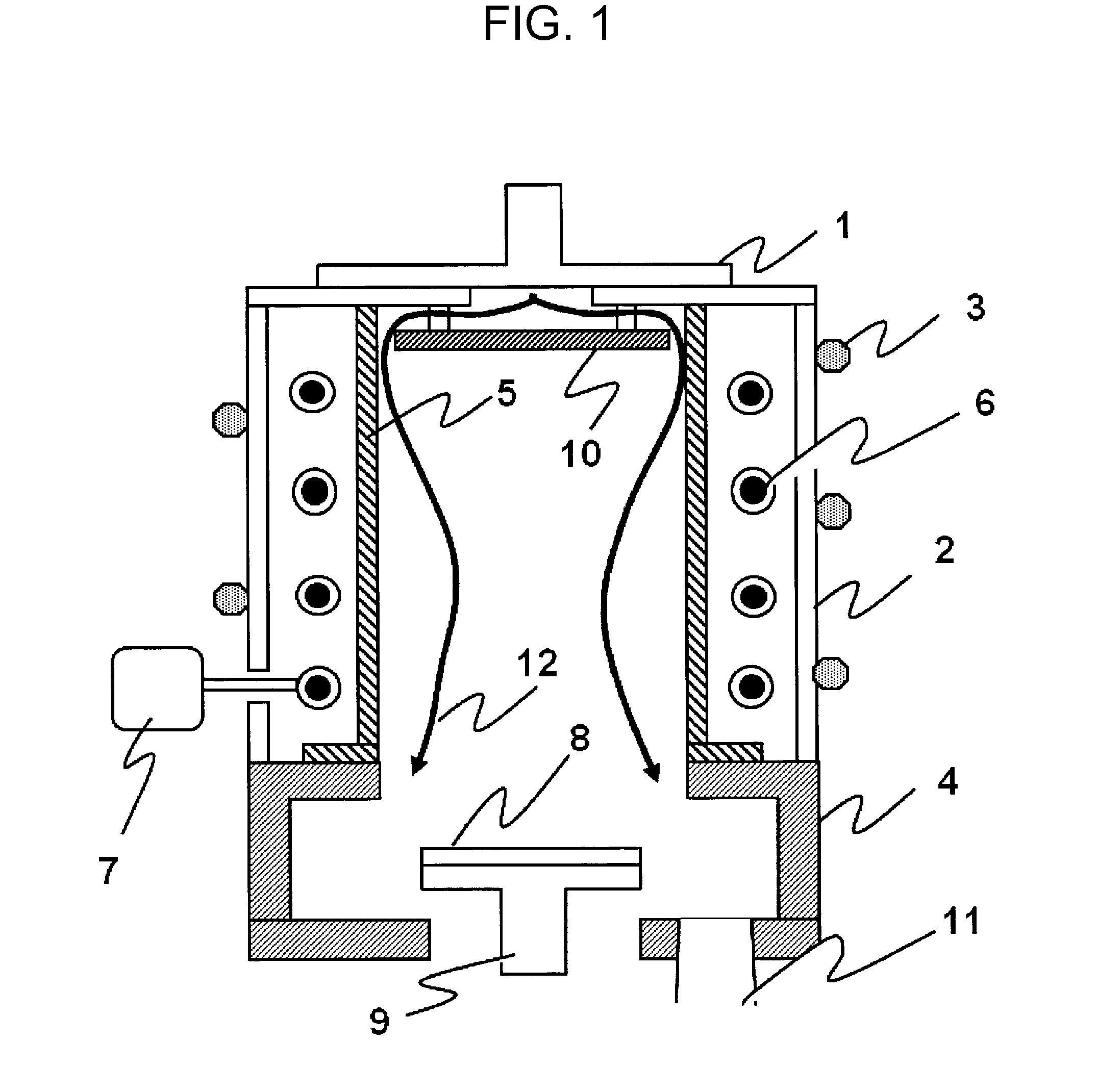
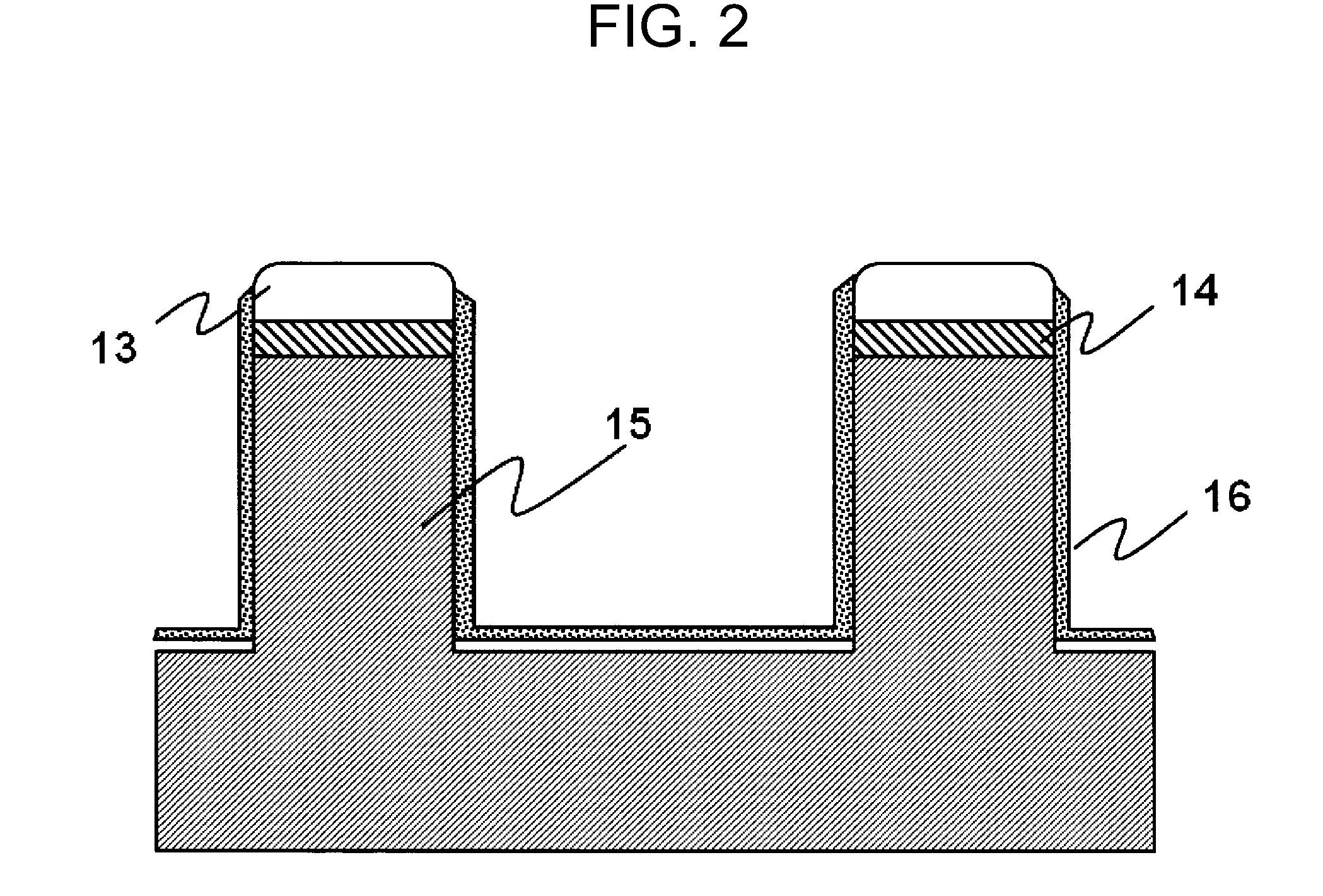
[0051]An ashing processing using the above-described plasma ashing apparatus will be described below. A wafer including an SiOC film 15 with a mask formed of a laminated structure of a resist mask 13 and a carbon hard mask 14 that has been etched by a plasma etching device is placed on the wafer stage 8 by a conveying unit (not shown).
[0052]Methane (CH4) gas 19 and argon (Ar) gas 17 are supplied to the quartz chamber 5 at a gas flow rate shown in Table 1, and the pressure inside the vacuum process chamber is adjusted to 200 Pa using an exhaust unit 11. Subsequently, 1000 W of radio-frequency electricity is supplied to the induction coils 6 to generate plasma and ashing is performed on the wafer placed on the wafer stage 8. The temperature of the stage during ashing of the wafer is controlled to be 300° C. Ashing is performed only for a predetermined period of time, and after that time has passed, the wafer placed on the wafer stage 8 is carried out from the plasma ashing apparatus b...
second embodiment
[0059]When the condition shown in Table 2 is used, ashing rate will be higher than the case where the condition shown in Table 1 is used. However, since a side wall of the Low-k film 15 including SiOC is directly exposed to the hydrogen (H+) radical 20 after a polymer attached to the pattern side wall as a result of plasma etching is removed, a film damage is likely to be exacerbated. Therefore, in order to achieve high ashing rate and to prevent a film damage, ashing may be performed with two steps including the condition shown in Table 2 as a first step and the condition shown in Table 1 as a second step, as shown in Table 3. Nevertheless, even in the case of using the condition shown in Table 2, both of high ashing rate and prevention of a film damage can be achieved if a gas flow rate of each of the argon (Ar) gas 17, the methane (CH4) gas 19, and hydrogen (H2) gas is optimized.
TABLE 3Radio-ArH2frequencyWafer stageCH4 gasgasgaselectricityPressuretemperatureStep(mL / min)(L / min)(W)...
PUM
| Property | Measurement | Unit |
|---|---|---|
| temperature | aaaaa | aaaaa |
| relative dielectric constant | aaaaa | aaaaa |
| temperature | aaaaa | aaaaa |
Abstract
Description
Claims
Application Information


