HFET with low access resistance

a technology of access resistance and transistor, which is applied in the direction of semiconductor devices, basic electric elements, electrical apparatus, etc., can solve the problems of discontinuity in the channel doping modulation, the maximum rf performance, and the difficulty of making the device operate in enhancement mode, so as to reduce the dispersion phenomenon associated with the effect of specific on resistance, reduced specific on resistance, and improved control of the transport properties of the devi

Inactive Publication Date: 2013-02-07
QUALCOMM INC
View PDF7 Cites 35 Cited by
  • Summary
  • Abstract
  • Description
  • Claims
  • Application Information

AI Technical Summary

Benefits of technology

[0022]The present invention describes a transistor based on a Hetero junction FET structure, where the access regions have been removed so as to effectively obtain a lower specific on-resistance, and a higher control on the transport properties of the device, drastically reducing the dispersion phenomena associated with these regions. The present invention can be realized both with polar and non-polar (or semi-polar) mater

Problems solved by technology

However the need to further improve on its general performance while reducing its cost is still a necessity that poses a significant challenge.
However, the reduction of Lg alone does not lead to maximum RF performance.
Another important limitation of these structures is the difficulty to make them operate in enhancement mode.
This causes a discontinuity in the doping modulation of the channel, adding two extra resistive paths in the channel.
Furthermore, since the carriers in the channel have to travel through the source-gate access region before reaching the controlled region underneath the gate, and similarly through the gate-drain access region before leaving the device, the illustrated structure suffers from high series resistance.
Nevertheless, due to trapping and de-trapping phenomena that can take place in the access regions, the device performance can be affected by dispersion phenomena, which represent one of the most important reliability issues in HEMT devices.
HEMT employing polar materials such as GaN and III-Nitride alloys oriented along the direction, present similar limitations.
I

Method used


Image

  • HFET with low access resistance
  • HFET with low access resistance
  • HFET with low access resistance

Examples


Embodiment Construction

A FIG. 4

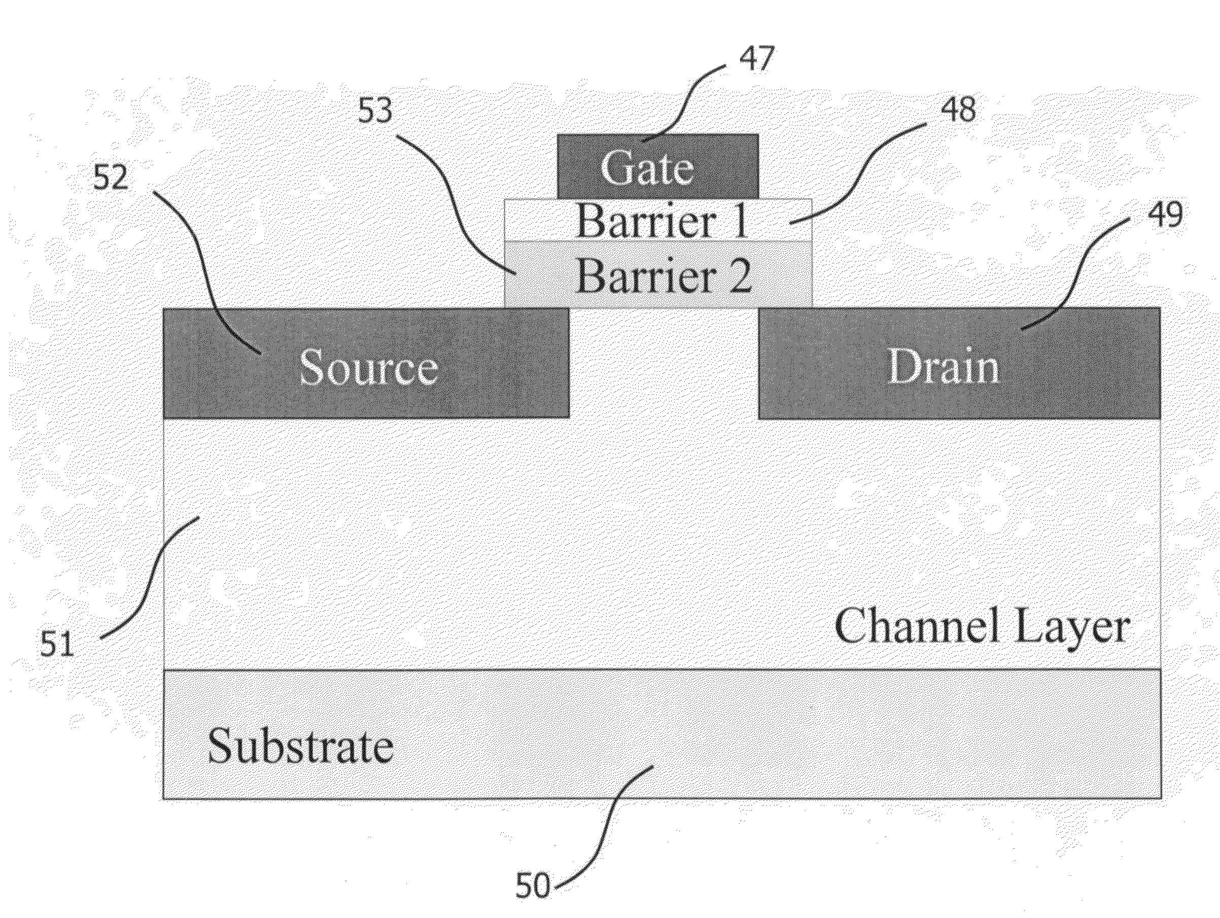
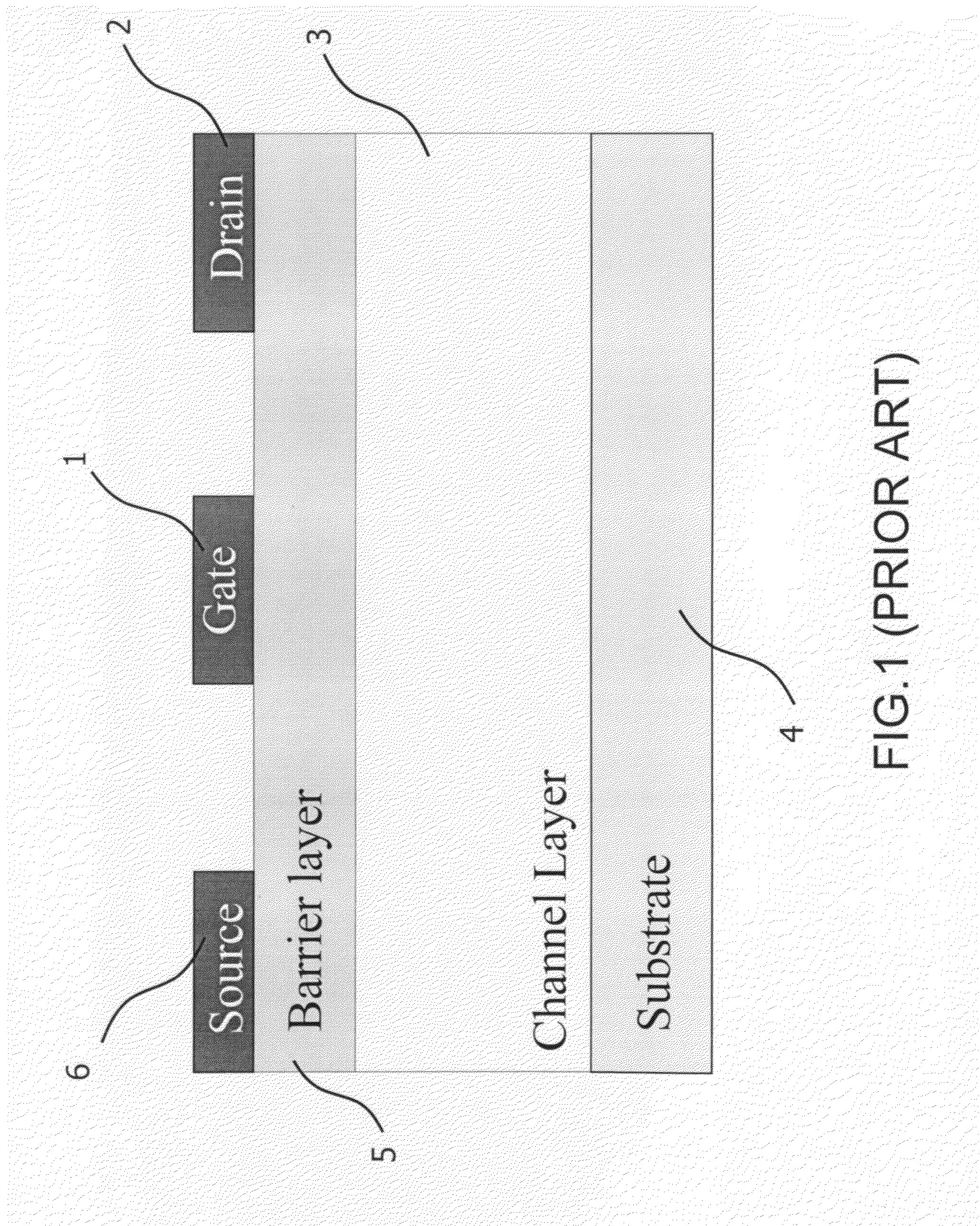
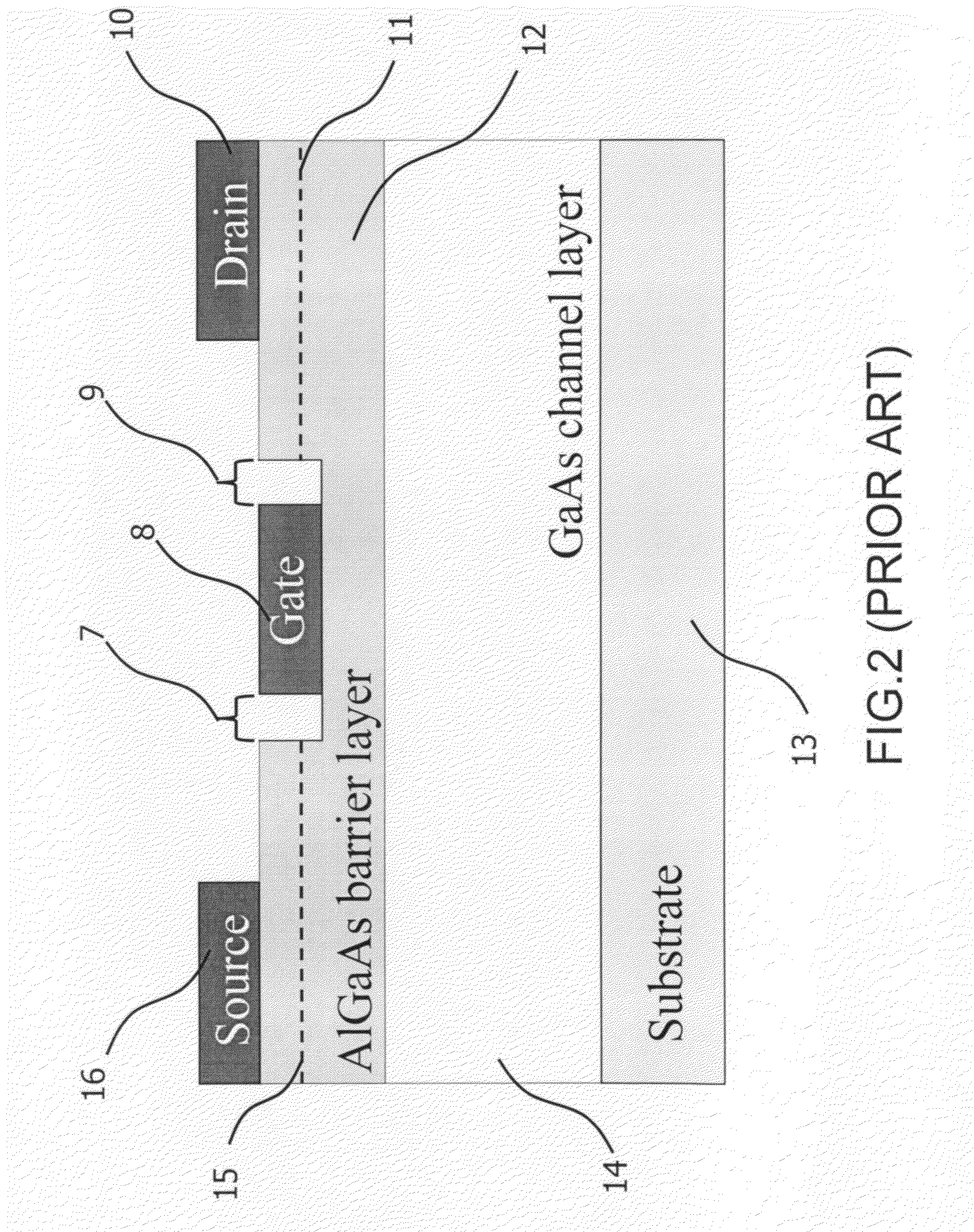
[0072]FIG. 4 is showing a Hetero-structure FET (HFET) device according to the preferred embodiment of the invention. The metallic or n+-type semiconductor regions 28 and 25 formed directly into the channel layer 27, define the source and the drain of the transistor. Regions 24 corresponds to the barrier layer of the device, and the channel layer 27 is the region where the electron (or hole)—channel is formed. Region 23, which can be formed using semiconductor materials or metal, corresponds to the gate of the device. As it can be seen, differently from the conventional HEMT structure of FIG. 1, no access regions can be identified in the device.

[0073]If the desired device is an n-channel HFET, the channel region should have an electron affinity greater with respect to the barrier layer 24, in order to confine the carrier transport inside the layer 27 during the normal operation of the device. The gate region 23 instead, can be built with the same, greater or lower electron af...


PUM


Abstract

A novel semiconductor power transistor is presented. The semiconductor structure is simple and is based on a Hetero-structure FET structure, where the access regions have been eliminated so as to effectively obtain a lower specific on-resistance, and a higher control on the transport properties of the device, drastically reducing the dispersion phenomena associated with these regions. The present invention can be realized both with polar and non-polar (or semi-polar) materials, without requiring delta doping implantation. It can be fabricated as an enhancement or depletion mode device with much higher control on the device threshold voltage with respect to state-of-the-art HFET devices, and achieving superior RF switching performance. Furthermore, due to the absence of access regions, enhancement mode devices can be realized without discontinuity in the channel conductivity, which results in an even lower on-resistance.

Description

BACKGROUND OF THE INVENTION[0001]1. Field of the Invention[0002]The present invention is in the field of semiconductor structures. The present invention is further in the field of semiconductor structures of transistor devices. The present invention further relates to the field of integrated devices and circuits. The implementation is not limited to a specific technology, and applies to either the invention as an individual component or to inclusion of the present invention within larger systems which may be combined into larger integrated circuits.[0003]2. Brief Description of Related Art[0004]The semiconductor transistor is the most important component for large integrated circuits. In the last three decades, field effect transistors (FETs) used in current integrated circuit process technologies have undergone a continuous shrinking of the semiconductor area needed for elementary components, and new materials including III-V and II-VI semiconductor compounds have been introduced t...

Claims


Application Information

Patent Timeline
IPC IPC(8): H01L29/778H01L21/335
CPCH01L29/267H01L29/66462H01L29/2003H01L29/7786H01L29/7787H01L29/7783H01L29/1066
Inventor MARINO, FABIO ALESSIOMENEGOLI, PAOLO
Owner QUALCOMM INC
Why Eureka
Try Eureka