Method of forming a self-aligned contact opening in MOSFET

a contact opening and self-aligning technology, applied in the field of mosfet technology of semiconductor, can solve the problems of difficult to achieve any of these dimensions without complicating process technology, limited cell pitch reduction of mosfet, and difficulty in reducing any of these dimensions, so as to reduce the cell pitch without increasing process complexity, the effect of easy control of the contact opening dimension

Active Publication Date: 2013-02-28
SINOPOWER SEMICON
View PDF3 Cites 11 Cited by
  • Summary
  • Abstract
  • Description
  • Claims
  • Application Information

AI Technical Summary

Benefits of technology

[0010]An object of this invention is to provide a method to form a self-aligned contact opening, which reduces the contact opening dimension and the contact mi

Problems solved by technology

However, reducing the cell pitch of MOSFETs is limited not only by the MOSFET cell structure but also the specific process to fabricate the MOSFET.
Furthermore, reducing the cell pitch is made further difficult by the limitations of the manufacturing process technology such as the minimum critical dimensions that the lithography tools can achieve, the minimum required spacing between different cell regions as dictated by the design rules, and the misalignment tolerances.
Reducing any of these dimensions without complicating the process technology i

Method used


Image

  • Method of forming a self-aligned contact opening in MOSFET
  • Method of forming a self-aligned contact opening in MOSFET
  • Method of forming a self-aligned contact opening in MOSFET

Examples


Embodiment Construction

[0023]The detailed explanation of the present invention is described as following. The described preferred embodiments are presented for purposes of illustrations and descriptions, and they are not intended to limit the scope of the present invention.

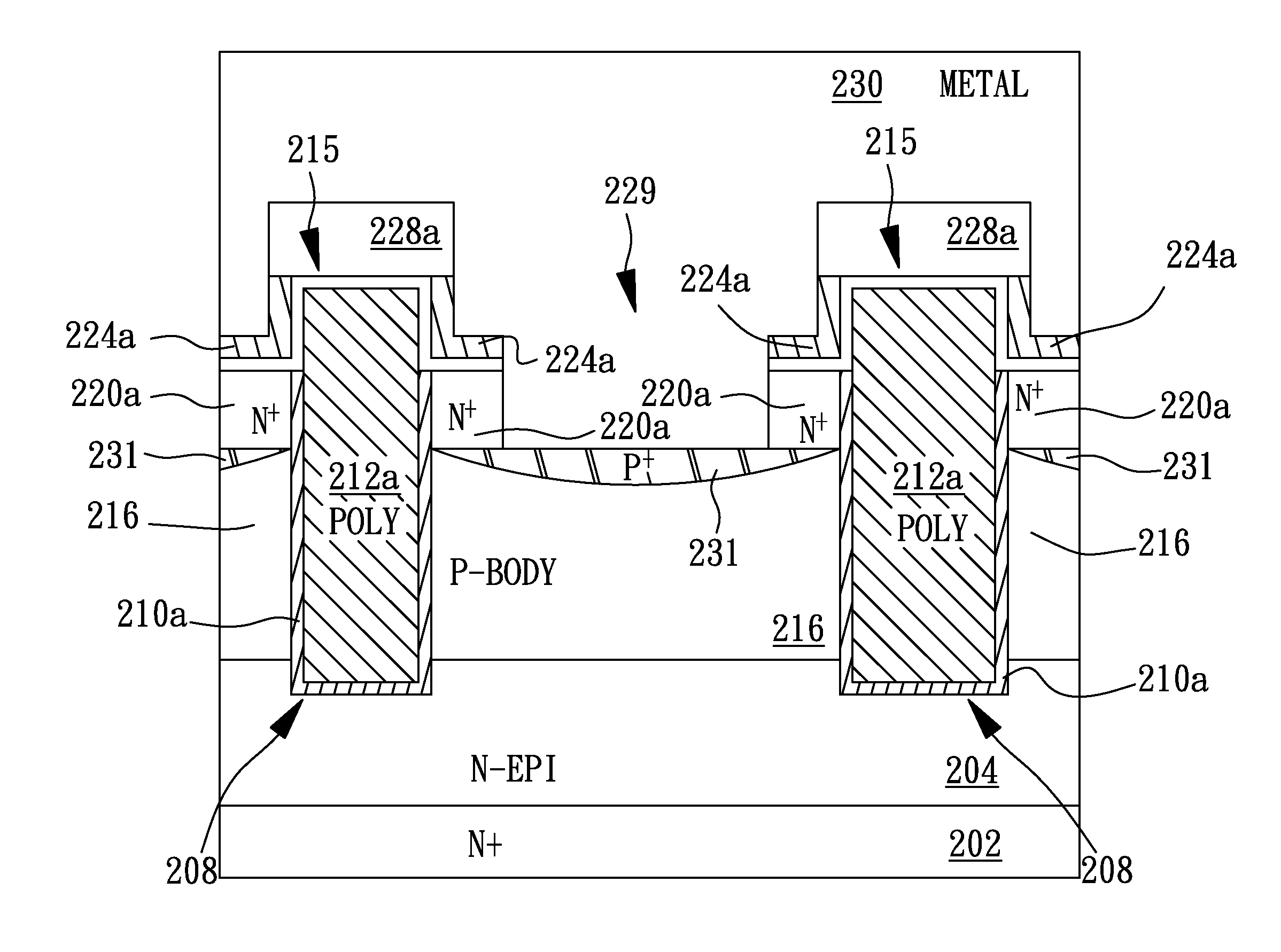
[0024]One embodiment of the present invention is a method to form an opening on a semiconductor substrate having two projecting portions, which can be applied to the process of manufacturing many different semiconductor device or structure such as, but is not limited to, a MOSFET device for forming a contact opening in the MOSFET.

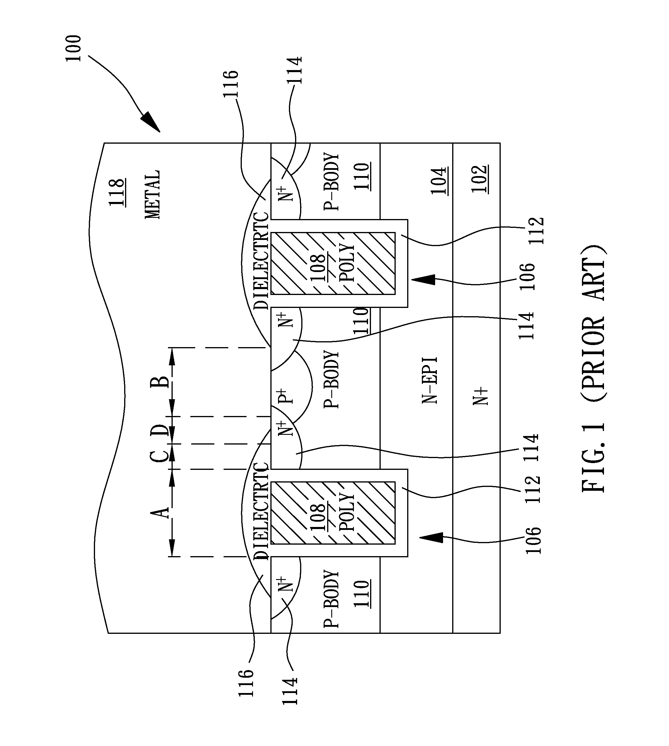
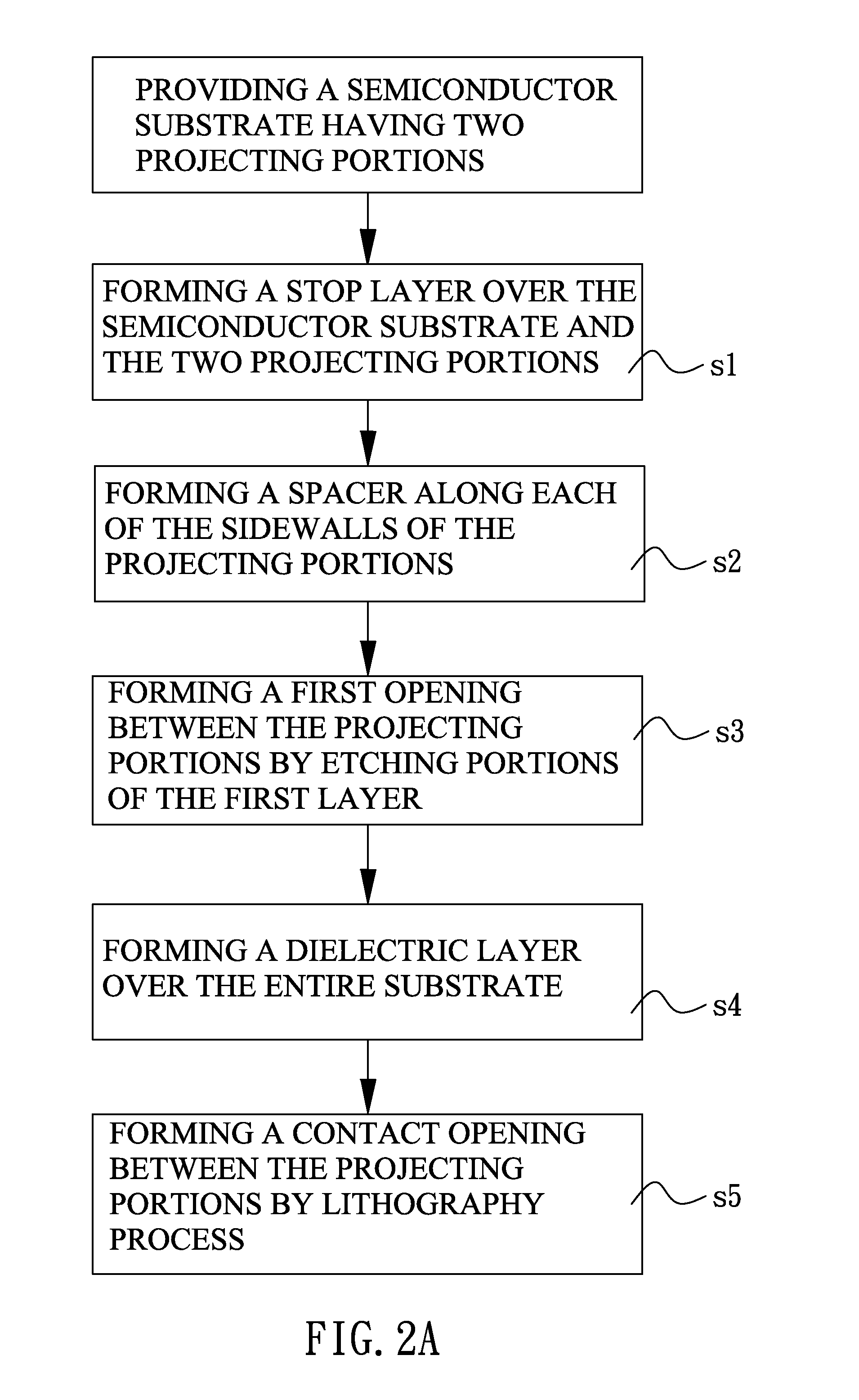
[0025]In one embodiment, the method of forming a self-aligned contact opening in a semiconductor substrate having two projecting portions according to the present invention comprises the following steps as shown in FIG. 2A. In step s1, form a stop layer over the semiconductor substrate extending over the two projecting portions. In step s2, form a spacer along each of the sidewalls of the projection portions as...


PUM


Abstract

A method of forming a contact opening in a semiconductor substrate is presented. A plurality of trench gates each having a projecting portion are formed in a semiconductor substrate, and a stop layer is deposited over the semiconductor substrate extending over the projecting portions, wherein each portion of the stop layer along each of the sidewalls of the projecting portions is covered by a spacer. By removing the portions of the stop layer not covered by the spacers by utilizing a relatively higher etching selectivity of the stop layer to the spacers, the openings between adjacent projecting portions with an L-type shape on each sidewall can be formed, and a lithography process can be performed to form self-aligned contact openings thereafter.

Description

FIELD OF THE INVENTION[0001]The present invention relates to semiconductor MOSFET technology, and in particular, to a trench MOSFET having self-aligned features.BACKGROUND OF THE INVENTION[0002]Power MOSFETs (metal oxide semiconductor field effect transistors) are well known in the semiconductor industry. One variety of power MOSFETs is the vertically-conducting trench MOSFET. A cross-section view of such a MOSFET is shown in FIG. 1, wherein MOSFET 100 has trenches 106 each including a poly-silicon gate 108 insulated from body regions 110 by a gate dielectric 112; source regions 114 flank each side of the trenches 106; dielectric layer 116 insulates the gates 108 from an overlay metal layer 118; and substrate region 102 forms the drain of MOSFET 100.[0003]When MOSFET 100 is in the on state, current flows vertically between the source regions 114 and the substrate 102; and the current is a function of the drain to source resistance (Rdson). To improve the current capability of the MO...

Claims


Application Information

Patent Timeline
IPC IPC(8): H01L29/78H01L21/336H01L21/3105
CPCH01L29/41741H01L29/41766H01L29/41775H01L29/7813H01L29/66727H01L29/66734H01L29/66719
Inventor TAI, SUNG-SHANYEH, TENG-HAOCHEN, CHIA-HUI
Owner SINOPOWER SEMICON
Why Eureka
Try Eureka