Diffused cap layers for modifying high-k gate dielectrics and interface layers

US20130052814A1Active Publication Date: 2013-02-28TOKYO ELECTRON LTD

Image

  • Diffused cap layers for modifying high-k gate dielectrics and interface layers
  • Diffused cap layers for modifying high-k gate dielectrics and interface layers
  • Diffused cap layers for modifying high-k gate dielectrics and interface layers

Examples


Embodiment Construction

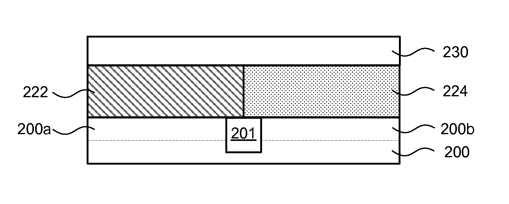
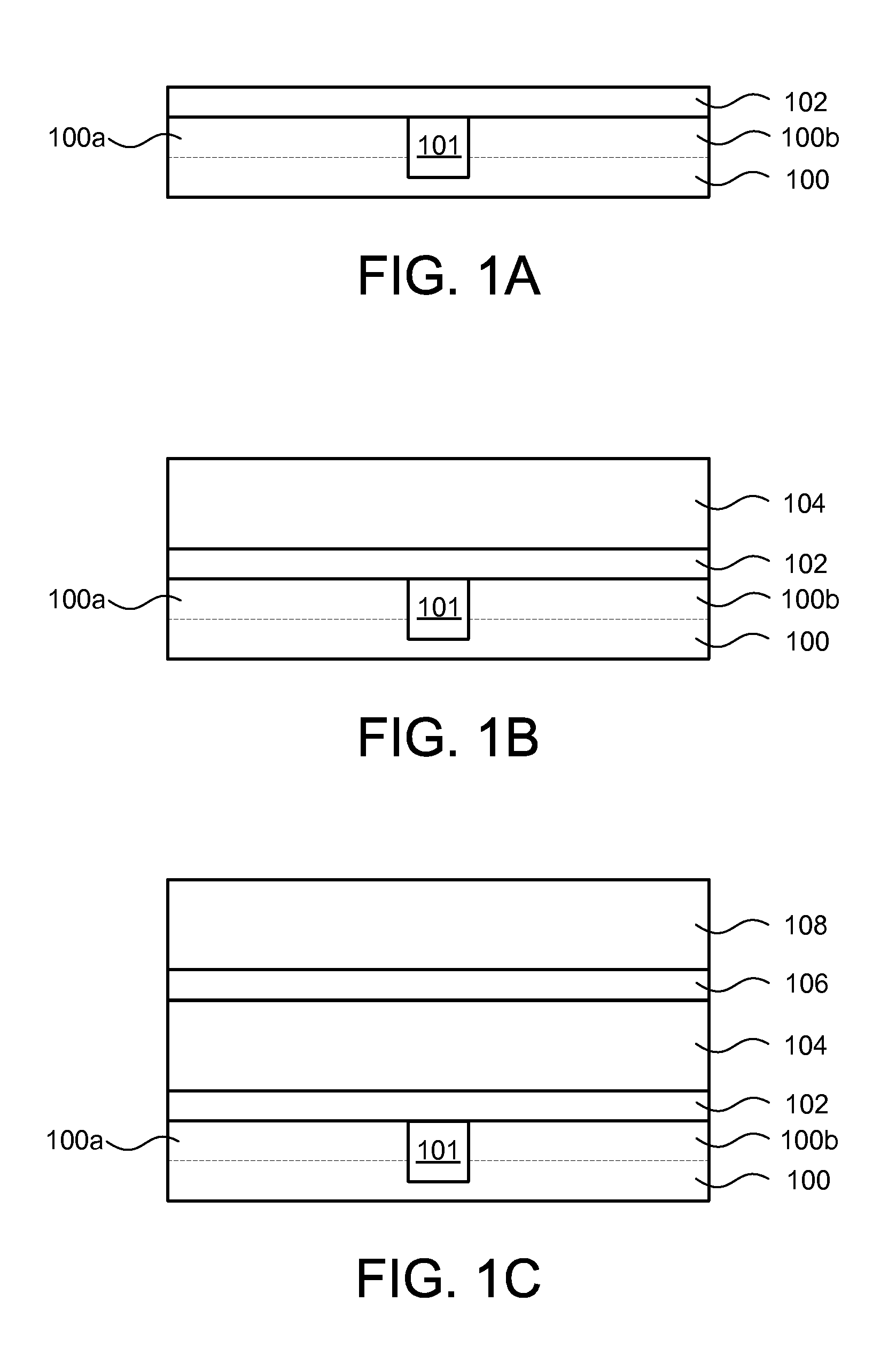
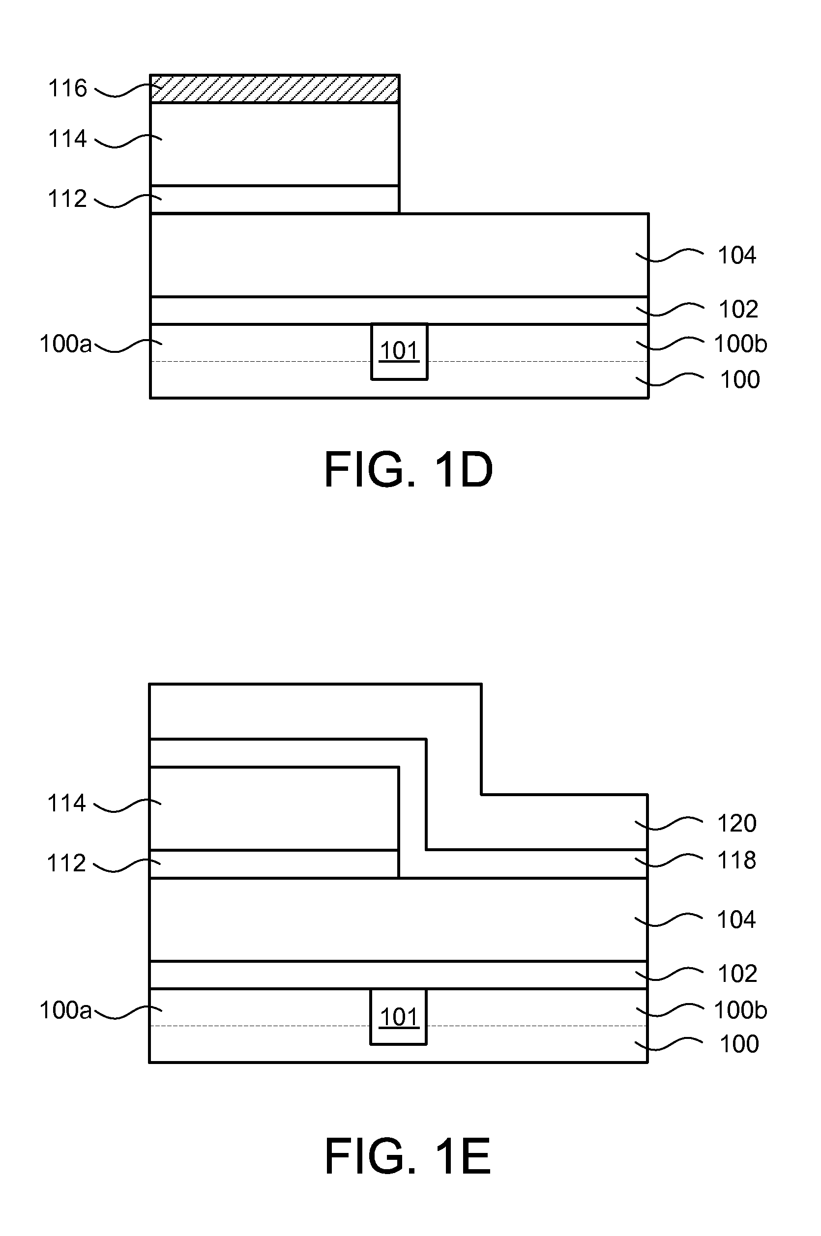
[0012]Embodiments of the invention describe a gate stack having a gate electrode film over a high-k film, and methods of manufacturing the same. In particular, a semiconductor device and a method for forming NMOS and PMOS transistors are disclosed in various embodiments, where the method combines an ultra-thin or zero thickness interface layer, a high-k film diffused with chemical elements that shift the threshold voltage that is appropriate for the NMOS, PMOS, or both NMOS and PMOS device regions, and a gate electrode on the high-k film. According to embodiments of the invention, first and second cap layers are formed on the high-k film over NMOS and PMOS device regions to provide chemical elements that can diffuse into the NMOS device regions, into the PMOS device regions, or into both the NMOS and PMOS device regions during a heat-treating process. The heat-treating process further reduces the thickness or eliminates an interface layer (e.g., SiO2) underneath the high-k film by o...


PUM


Abstract

Method of forming a semiconductor device includes providing a substrate with defined NMOS and PMOS device regions and an interface layer on the NMOS and PMOS device regions, depositing a high-k film on the interface layer, depositing a first cap layer on the high-k film, and removing the first cap layer from the high-k film in the PMOS device region. The method further includes depositing a second cap layer on the first cap layer in the NMOS device region and on the high-k film in the PMOS device region, performing a heat-treating process to diffuse a first chemical element into the high-k film in the NMOS device region and to reduce or eliminate the interface layer by oxygen diffusion from the interface layer into the second cap layer, removing the first and second cap layers from the high-k film, and depositing a gate electrode film over the high-k film.

Description

FIELD OF INVENTION[0001]The present invention relates to semiconductor devices, and more particularly to a gate stack having a gate electrode over a high-k gate dielectric, and methods of manufacturing the same.BACKGROUND OF THE INVENTION[0002]As the size and scaling of semiconductor device technology is reduced, aspects of device design and fabrication that previously gave rise to only second-order effects in long-channel devices can no longer be ignored. For example, the reduced scaling of channel length and gate oxide thickness in a conventional metal-oxide-semiconductor (MOS) transistor exacerbates problems of polysilicon gate depletion, high gate resistance, high gate tunneling leakage current and device (i.e., boron) penetration into the channel region of the device. As a result, CMOS technology is increasingly replacing silicon dioxide gate dielectrics and polysilicon gate conductors with high dielectric constant (high-k) gate dielectrics in combination with metal gate electr...

Claims


Application Information

Patent Timeline
28 Feb 2013
Publication
US20130052814A1
IPC
H01L21/28
CPC
H01L21/823842; H01L21/823857; H01L21/28079; H01L21/28088; H01L29/517; H01L21/28185; H01L29/495; H01L29/4966
Inventors
CLARK, ROBERT D.