Radiation-Emitting Component with a Semiconductor Chip and a Conversion Element and Method for the Production Thereof

a technology of conversion elements and semiconductor chips, which is applied in the direction of semiconductor/solid-state device manufacturing, semiconductor devices, electrical devices, etc., can solve problems such as affecting achieve the effects of improving the efficiency of components, improving the refractive index of matrix materials, and improving heat dissipation

Inactive Publication Date: 2013-03-07
OSRAM OPTO SEMICONDUCTORS GMBH & CO OHG +1
View PDF1 Cites 6 Cited by
  • Summary
  • Abstract
  • Description
  • Claims
  • Application Information

AI Technical Summary

Benefits of technology

[0007]In one aspect, the present invention provides a radiation-emitting component which is distinguished by improved dissipation of the heat arising during operation of the component by the matrix material, consequent improved efficiency of the component and simultaneously by an elevated refractive index of the matrix material.
[0020]The luminescent material of the conversion element is embedded in the matrix material of tellurium-containing glass. Glass advantageously exhibits better thermal conductivity than the silicone which is conventionally used, whereby dissipation of the heat arising during operation by the matrix material is advantageously increased. In this manner, the heat arising during operation, in particular that arising during operation by heating of the luminescent material in the conversion element, may be efficiently dissipated via the matrix material, so advantageously increasing the efficiency of the luminescent material and consequently the efficiency of the component.
[0028]In a further preferred embodiment, the matrix material comprises at least one additional element which increases the refractive index of the matrix material. Refractive index-increasing compounds known to a person skilled in the art, such as for example La2O3, may for example be added to the glass.
[0032]In a further preferred development, the matrix material is a low-melting material. For the purposes of the present application, a low-melting material is considered to be a material which softens at a temperature of at most 350° C. This advantageously makes it possible to join the conversion element directly to the semiconductor chip by the bond being created between the conversion element and semiconductor chip at at most 350° C., wherein at such temperatures the semiconductor chip suffers no damage when the conversion element is applied onto the radiation exit face of the semiconductor chip. A bonding wire, for example a gold wire, which is used for electrical contacting of the semiconductor chip may be completely or partially embedded in the conversion element.

Problems solved by technology

Silicone, however, exhibits poor thermal conductivity, which may result in the luminescent material heating up when the component is in operation, so disadvantageously impairing the efficiency of the component.

Method used


Image

  • Radiation-Emitting Component with a Semiconductor Chip and a Conversion Element and Method for the Production Thereof
  • Radiation-Emitting Component with a Semiconductor Chip and a Conversion Element and Method for the Production Thereof
  • Radiation-Emitting Component with a Semiconductor Chip and a Conversion Element and Method for the Production Thereof

Examples


Embodiment Construction

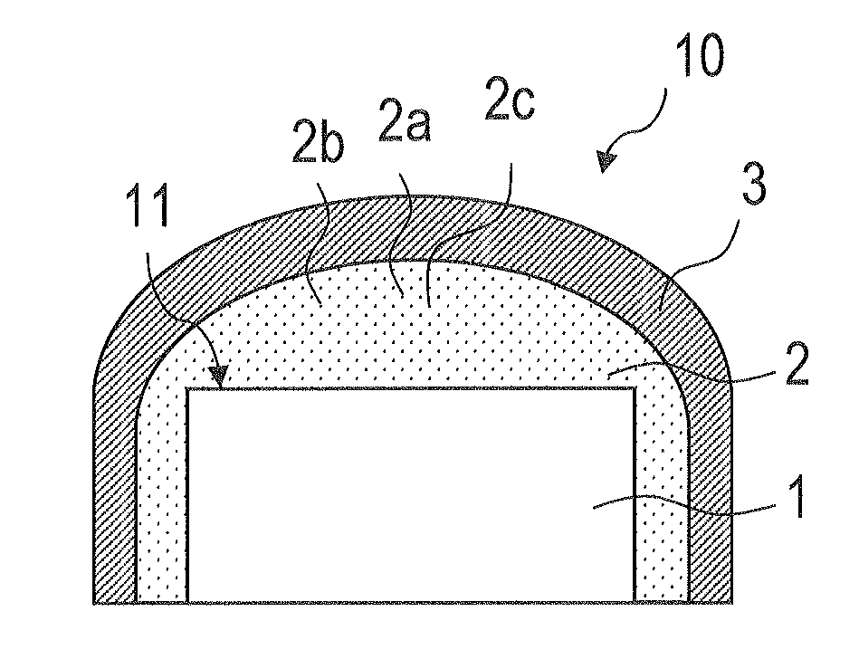
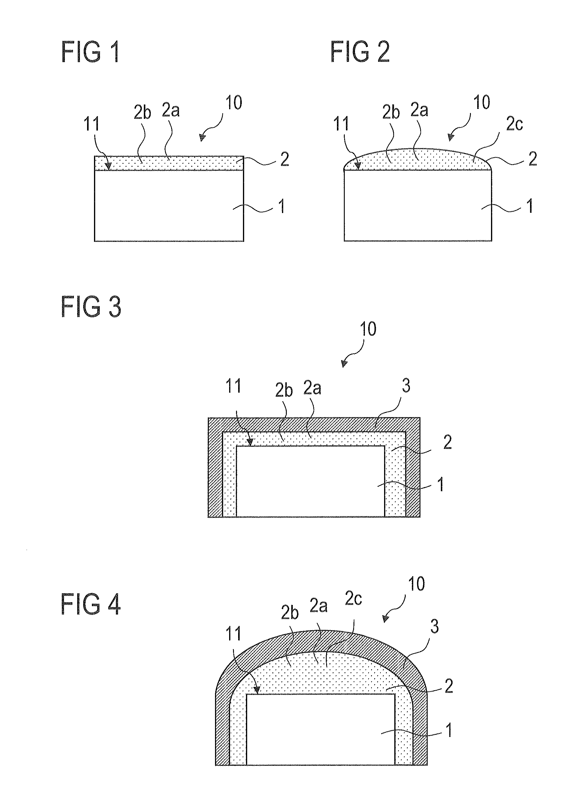
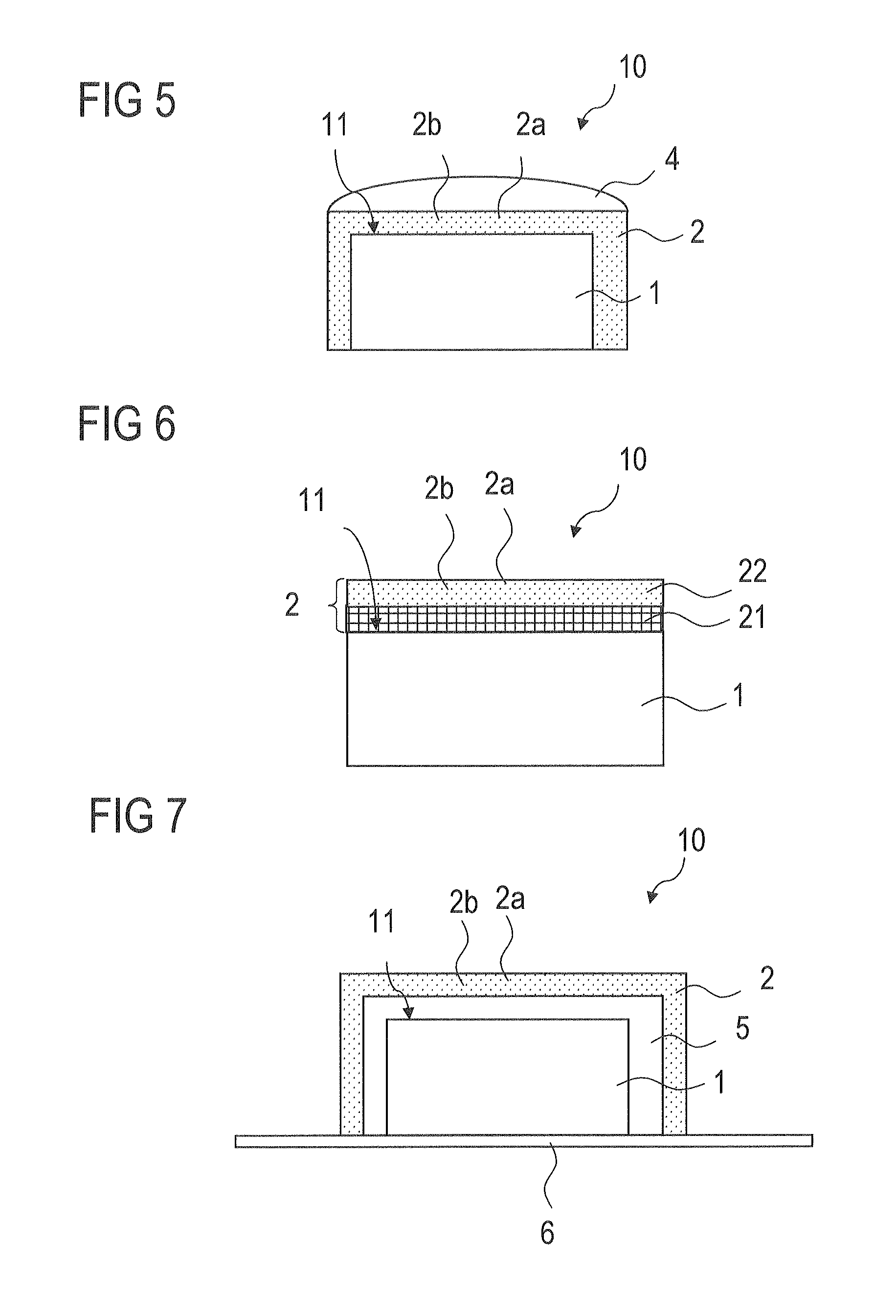
[0052]FIG. 1 shows a radiation-emitting component 10 which comprises a semiconductor chip 1 and a conversion element 2.

[0053]A radiation-emitting component should substantially be taken to mean a component which is suitable for emitting radiation when in operation. In particular, radiation emission in operation proceeds in such components by means of electrical contacting of the components.

[0054]The semiconductor chip 1 is preferably an LED chip (LED: light-emitting diode). The semiconductor chip 1 is preferably a thin-film LED. In a thin-film LED, the production substrate, on which the layer stack for the semiconductor chip 1 was produced, in particular deposited, is removed in zones or completely.

[0055]The semiconductor chip 1 comprises an active layer suitable for generating electromagnetic radiation. The active layer of the semiconductor chip 1 comprises a pn-junction, a double heterostructure, a single quantum well structure (SQW) or a multi quantum well structure (MQW) for gen...


PUM


Abstract

A radiation-emitting component includes a semiconductor chip and a conversion element. The semiconductor chip includes an active layer suitable for generating electromagnetic radiation and a radiation exit face. The conversion element includes a matrix material and a luminescent material. The conversion element is arranged downstream of the radiation exit face of the semiconductor chip. The matrix material comprises at least 40 wt. % tellurium oxide and is free of boron trioxide and / or germanium oxide. A method for producing such a radiation-emitting component is furthermore stated.

Description

[0001]This patent application is a national phase filing under section 371 of PCT / EP2011 / 052851, filed Feb. 25, 2011, which claims the priority of German patent application 10 2010 009 456.0, filed Feb. 26, 2010, each of which is incorporated herein by reference in its entirety.TECHNICAL FIELD[0002]The invention relates to a radiation-emitting component with a semiconductor chip and a conversion element. The invention further relates to a method for producing a radiation-emitting component.BACKGROUND[0003]Radiation-emitting components with a conversion element are known, for example, from document WO 97 / 50132. These components contain a semiconductor body which emits light (primary light) when in operation and a conversion element with a luminescent material which converts a proportion of the primary light into another wavelength range (secondary light). The color appearance of the light emitted by such a semiconductor component is the result of additive color mixing of primary ligh...

Claims


Application Information

Patent Timeline
Patent Type & Authority Applications(United States)
IPC IPC(8): H01L33/26H01L33/50
CPCH01L33/50H01L33/56H01L33/507H01L33/508H01L33/501H01L2924/0002H01L33/502H01L2924/00H01L33/58
Inventor EBERHARDT, ANGELAWIRTH-SCHOEN, JOACHIMPOESL, EWALD
Owner OSRAM OPTO SEMICONDUCTORS GMBH & CO OHG
Why Eureka
Try Eureka