Optoelectronic device having an embedded electrode

a technology of optoelectronic devices and embedded electrodes, which is applied in the direction of thermoelectric devices, sustainable manufacturing/processing, and final product manufacturing, etc., can solve the problems of difficult integration of a sam layer in a diode stack such as shown in fig. 1

Inactive Publication Date: 2013-03-21
COMMISSARIAT A LENERGIE ATOMIQUE ET AUX ENERGIES ALTERNATIVES
View PDF1 Cites 10 Cited by
  • Summary
  • Abstract
  • Description
  • Claims
  • Application Information

AI Technical Summary

Benefits of technology

[0016]The invention aims at a high-performa

Problems solved by technology

However, such materials are easily oxidizable and have a high instability regarding oxygen and/or water.
On the anode side, there also is a mismatch between materials.
The integration of a SAM layer in a diode stack such as shown in FIG. 1 is difficult.
Indeed, since the SAM layer is to be grafted on the electrode material, it cannot be deposited on the organic materia

Method used


Image

  • Optoelectronic device having an embedded electrode
  • Optoelectronic device having an embedded electrode
  • Optoelectronic device having an embedded electrode

Examples


Embodiment Construction

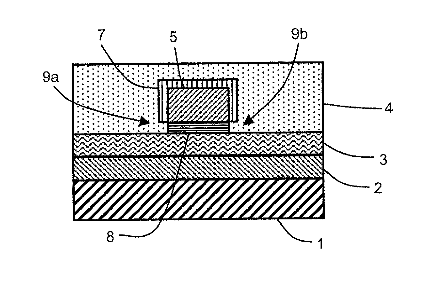
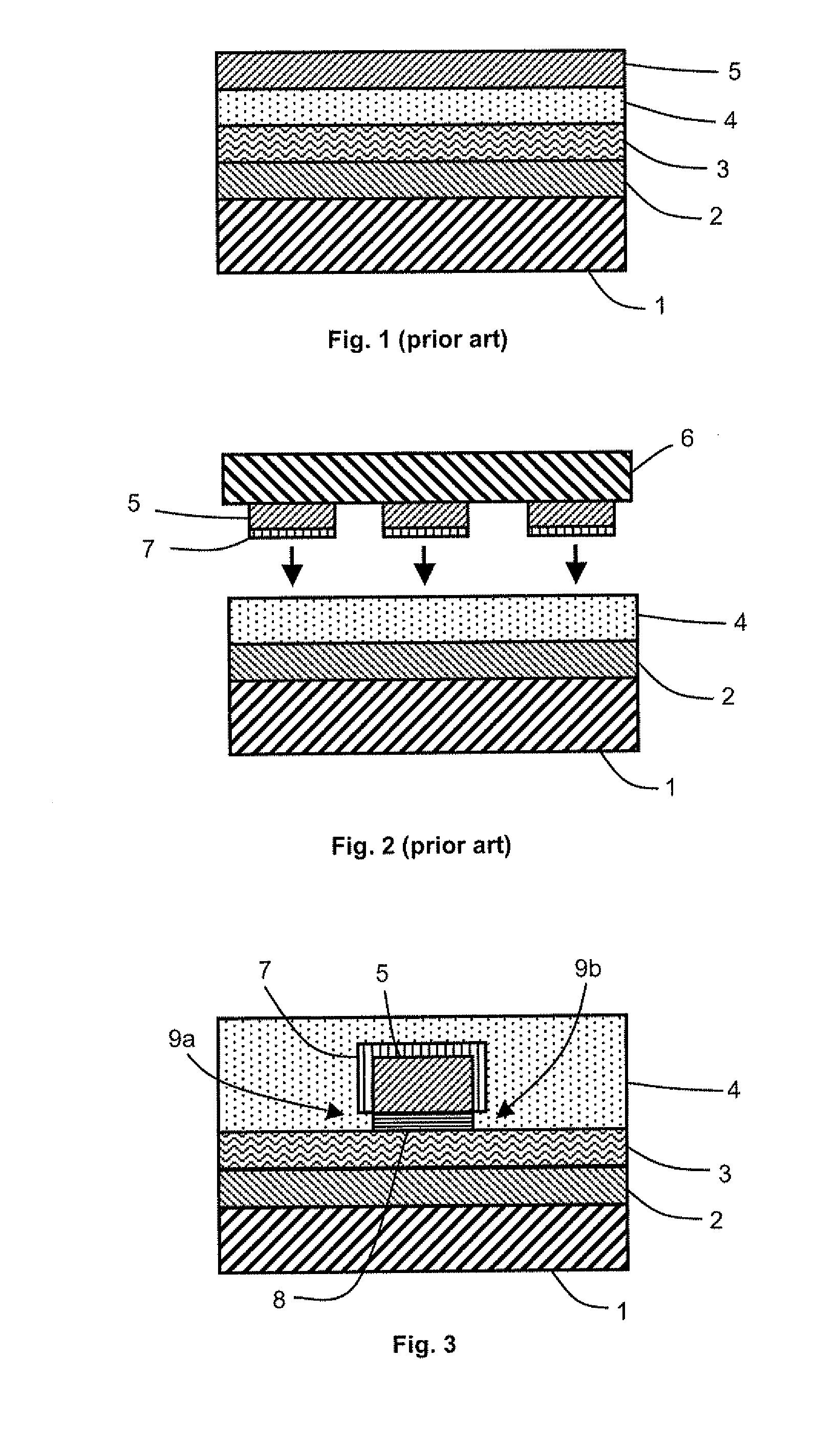
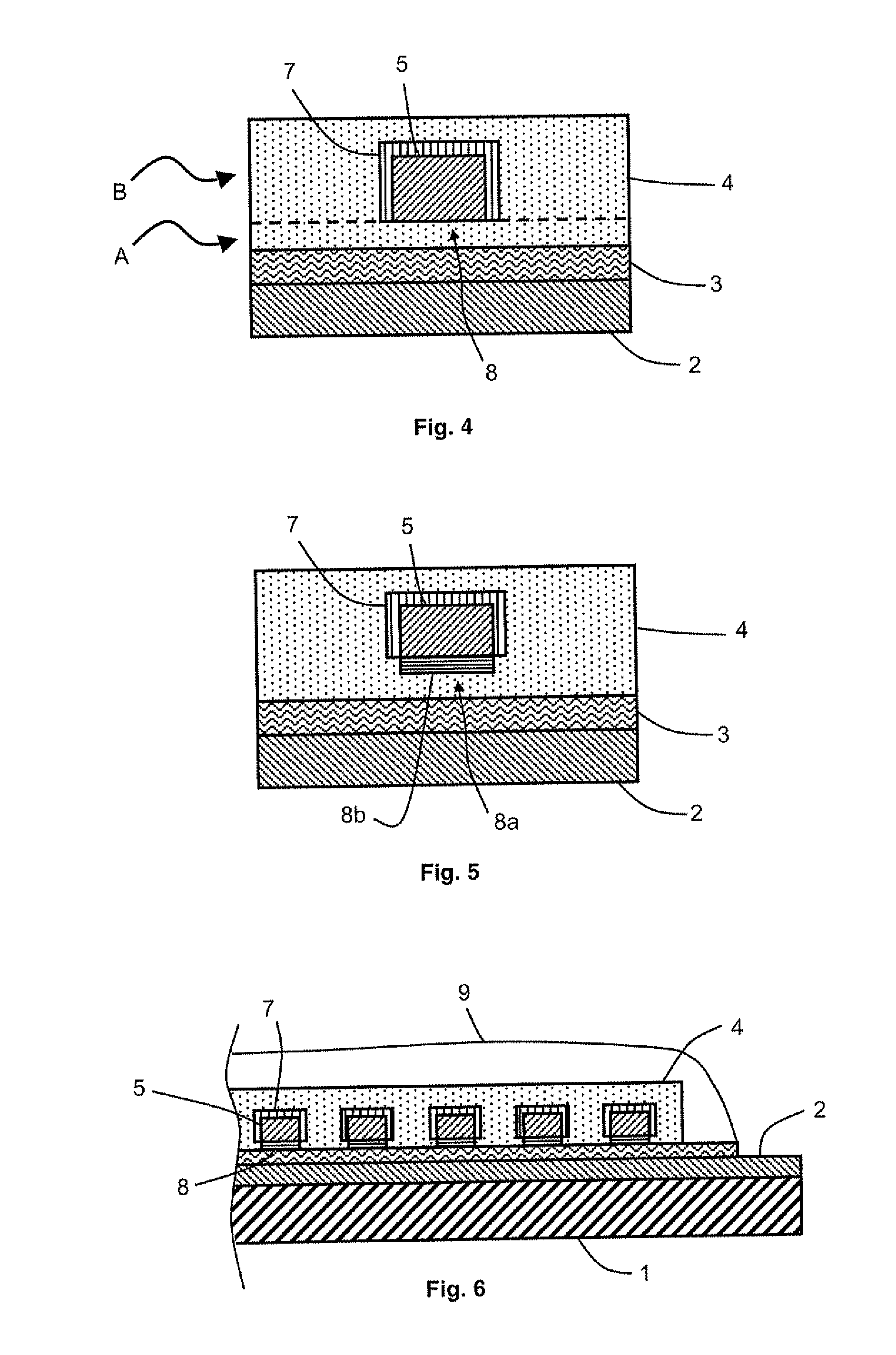
[0031]FIG. 3 shows an embodiment of an optoelectronic device having an embedded electrode.

[0032]The device comprises a first electrode 2 arranged on a substrate 1. The first electrode is preferably provided with a charge injection and transport layer 3.

[0033]The device also comprises a second electrode 5 arranged in front of the first electrode. Electrode 5 has a compact shape, and is located at the center of the device. Electrode 5 is located above electrode 2 and substrate 1 and is insulated from electrode 2 by a separation area 8.

[0034]A layer 4 made from an organic semiconductor material is arranged in electric contact with electrode 2, via injection layer 3, for example.

[0035]As mentioned previously, given the nature of electrode 5, the contact between electrode 5 and organic material 4 should be established by insertion of a SAM layer 7. Since layer 7 cannot be arranged on the lower surface of electrode 5 for reliability reasons, it is arranged on the other surfaces of electro...


PUM


Abstract

An optoelectronic device including a first electrode arranged on a substrate, a second electrode that includes a first surface facing the first electrode, and a semiconductor material layer that is in electric contact with the first and second electrodes. The second electrode includes a side wall that is adjacent to the first surface and is covered with the semiconductor material layer by the insertion of a self-assembled monolayer.

Description

BACKGROUND OF THE INVENTION[0001]The invention relates to a diode-type optoelectronic device using a semiconductor material.State of the art[0002]FIG. 1 schematically shows a conventional organic light-emitting diode (OLED) architecture. Such a diode comprises a stack of thin layers on a transparent glass substrate 1. The stack generally comprises a first electrode to 2 (anode), a hole injection and transport layer 3, an organic semiconductor material layer 4, and a second electrode 5 (cathode).[0003]Thus, in such a configuration, said to be vertical, electrodes 2 and 5 are placed on either side of layer 4, which has a thickness of approximately 150 nm.[0004]Electrode 2, on the substrate side, is generally made of indium tin oxide (ITO). ITO is a hole conductor and is transparent to the radiation emitted from organic layer 4. Layer 3, called injection layer, which is also transparent to the emission wavelength, promotes the injection of holes from the anode to the organic material a...

Claims


Application Information

Patent Timeline
IPC IPC(8): H01L51/50H01L51/42
CPCH01L51/441H01L51/5203H01L51/5221Y02E10/549H01L51/50H01L51/5088H01L51/42Y02P70/50H10K30/81H10K50/805H10K50/822H10K30/00H10K50/00H10K50/17H10K50/82H10K71/00
Inventor LAURENT, JEAN-YVESVERILHAC, JEAN-MARIE
Owner COMMISSARIAT A LENERGIE ATOMIQUE ET AUX ENERGIES ALTERNATIVES
Why Eureka
Try Eureka