Nanocrystalline copper indium diselenide (CIS) and ink-based alloys absorber layers for solar cells

a technology of ink-based alloys and absorber layers, which is applied in the direction of selenium/tellurium compunds, sustainable manufacturing/processing, and final product manufacturing, etc., can solve the problems of limiting the substrate upon, increasing throughput and increasing costs, and the nanoparticle synthesis process methods often suffer from the ease of scalable or controlling morphology and stoichiometry. , to achieve the effect of easy production

Inactive Publication Date: 2013-05-16
UNIV OF FLORIDA RES FOUNDATION INC +1
View PDF5 Cites 7 Cited by
  • Summary
  • Abstract
  • Description
  • Claims
  • Application Information

AI Technical Summary

Benefits of technology

[0008]Another embodiment of the invention is directed to a method to prepare the CIS comprising nanoparticles where a copper halide or its equivalent in a first solution, an indium halide or its equivalent in a second solution, and selenium, sulfur, or tellurium in a third solution are combined followed by heating to a temperature up to 150° C. to form a precipitate. The resulting CIS comprising nanoparticles can be washed. The solvents used for the first solution and second solution can be an alcohol. The solvent for the third solution can be an amine or a diamine. The solvents can be selected to allow the heat to be controlled by the temperature where the solv...

Problems solved by technology

The technical challenge is to synthesize CIS based absorber layers at high throughput and yield while maintaining good cell performance.
Currently practiced techniques for depositing CIS absorber layers, including evaporation, sputtering, and selenization of intermetallics, are carried out at higher temperatures, which limits the substrate upon which it is deposited, and for extended periods of time, which decreases...

Method used


Image

  • Nanocrystalline copper indium diselenide (CIS) and ink-based alloys absorber layers for solar cells
  • Nanocrystalline copper indium diselenide (CIS) and ink-based alloys absorber layers for solar cells
  • Nanocrystalline copper indium diselenide (CIS) and ink-based alloys absorber layers for solar cells

Examples


Embodiment Construction

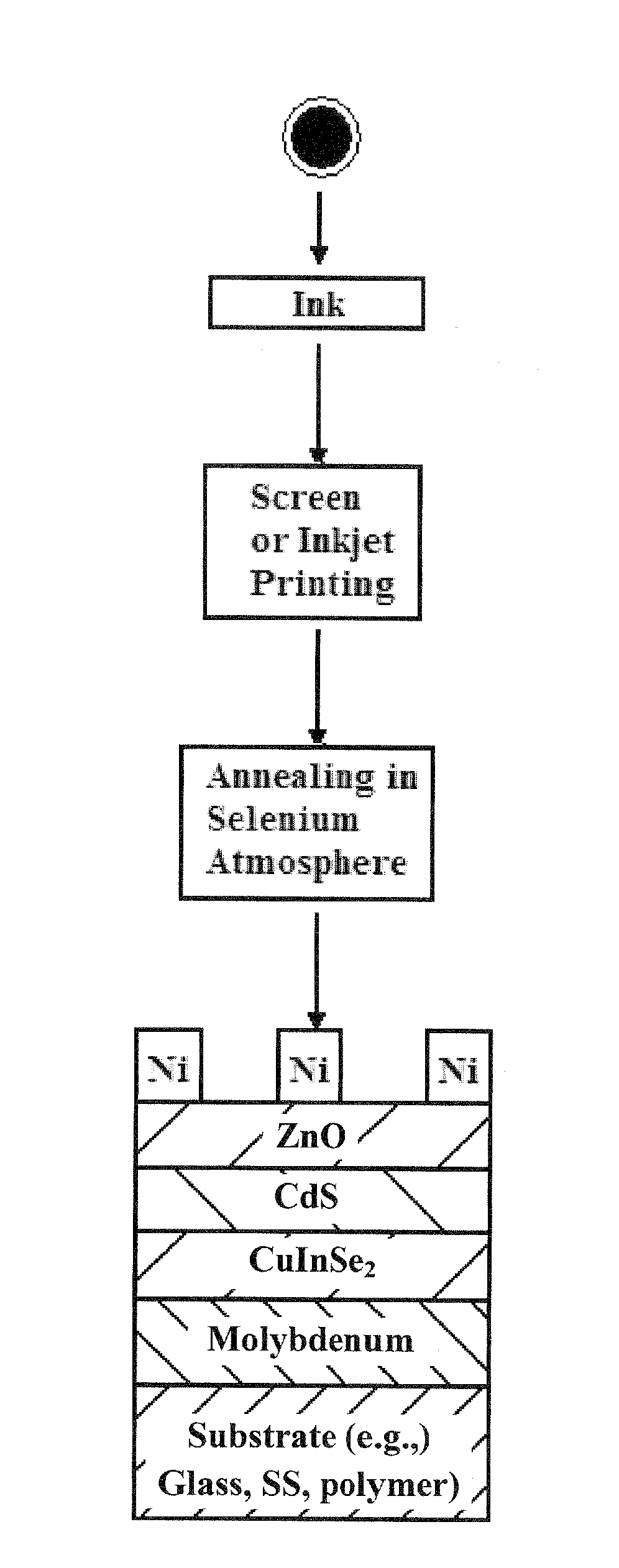
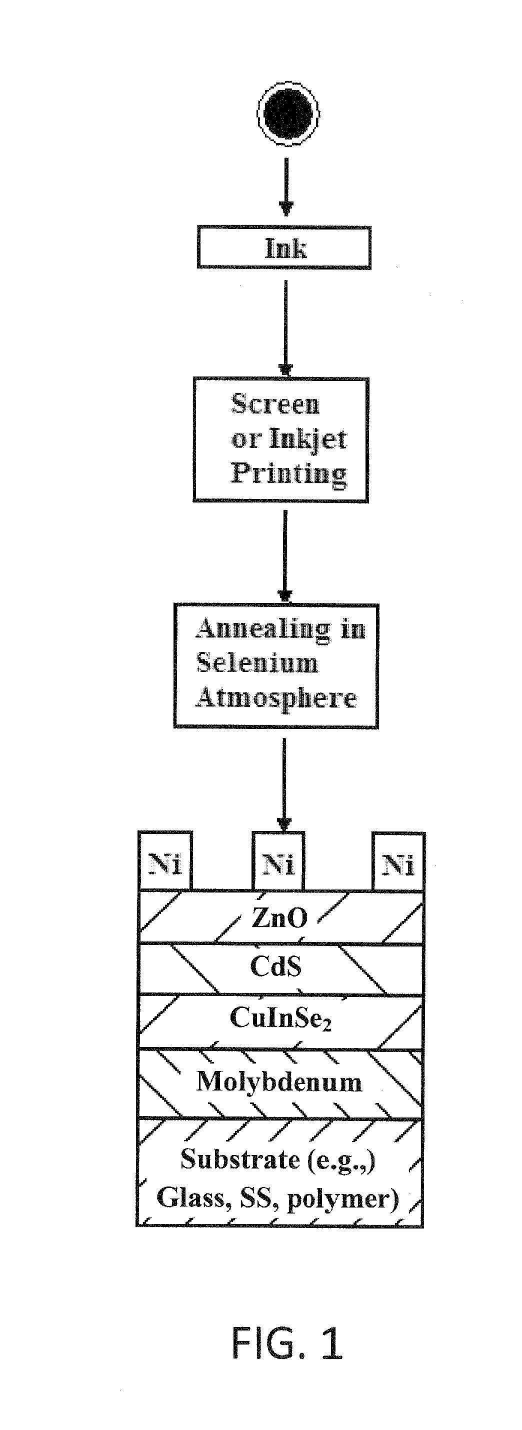
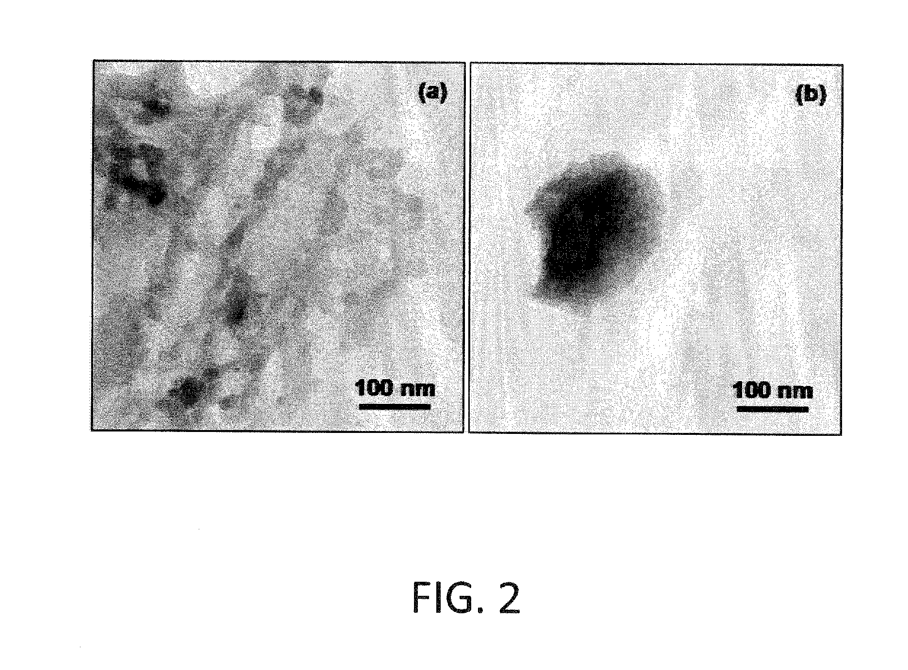
[0017]Embodiments of the invention are directed to a copper indium diselenide (CIS) comprising absorber layer from CIS comprising nanoparticles having a secondary phase comprising a compound that decomposes to a liquid, for example a copper selenide, for example CuSe2, CuSe, and or Cu3Se2 and a photovoltaic cell comprising the CIS comprising absorber layer. FIG. 1 give a schematic representation of CIS comprising nanoparticles, an Ink prepared from the CIS comprising nanoparticles, method steps to deposit the ink as a precursor layer and conversion of the precursor layer to a CIS comprising absorber layer for a photovoltaic device as exemplified at the bottom of the scheme. The CIS comprising nanoparticles according to an embodiment of the invention are copper selenide rich, which is achieved by growing the nanoparticles under conditions rich in copper ion and selenium. The copper selenide rich conditions results in the formation of the secondary phase during the process of forming ...


PUM


Abstract

Embodiments of the invention are to a copper indium diselenide (CIS) comprising nanoparticle where the nanoparticle includes a CIS phase and a second phase comprising a copper selenide. The CIS comprising nanoparticles are free of surfactants or binding agents, display a narrow size distribution and are 30 to 500 nm in cross section. In an embodiment of the invention, the CIS comprising nanoparticles are combined with a solvent to form an ink. In another embodiment of the invention, the ink can be used for screen or ink-jet printing a precursor layer that can be annealed to a CIS comprising absorber layer for a photovoltaic device.

Description

CROSS-REFERENCE TO RELATED APPLICATION[0001]The present application claims the benefit of U.S. Provisional Application Ser. No. 61 / 357,170, filed Jun. 22, 2010, which is hereby incorporated by reference herein in its entirety, including any figures, tables, or drawings.[0002]The subject invention was made with government support under the Department of Energy, Contract No. DE-FG36-08GO18069. The government has certain rights to this invention.BACKGROUND OF INVENTION[0003]Recently, copper indium diselenide (CIS) and related chalcopyrite alloys have been intensively studied worldwide as a promising material system for thin film photovoltaics owing to their unique structural and optoelectronic properties. CIS and its alloys have tremendous potential to reduce the manufacturing costs of thin film solar cells relative to that for crystalline silicon-based solar cells. The technical challenge is to synthesize CIS based absorber layers at high throughput and yield while maintaining good ce...

Claims


Application Information

Patent Timeline
IPC IPC(8): H01L31/18H01L31/032H01L31/0272
CPCH01L31/18H01L31/0272H01L31/0322Y10S977/773Y10S977/896Y10S977/824B82Y40/00C09D11/52H01L31/0749Y02E10/541Y02P70/50H01L31/0445
Inventor ANDERSON, TIMOTHY JAMESPARK, CHINHOKRISHNAN, RANGARAJANFARVA, UMME
Owner UNIV OF FLORIDA RES FOUNDATION INC
Why Eureka
Try Eureka