High-density p-doped quantum dot solar cell obtained by the active doping of inp and a production method therefor

a quantum dot and production method technology, applied in the field of quantum dot solar cells, can solve the problems of low efficiency of photovoltaic devices made of other materials, short lifespan, and adjustment of doping concentration, and achieve the effects of high purity p doping, excellent light absorption efficiency, and simple and easy method

Active Publication Date: 2013-05-16
KOREA RES INST OF STANDARDS & SCI
View PDF5 Cites 7 Cited by
  • Summary
  • Abstract
  • Description
  • Claims
  • Application Information

AI Technical Summary

Benefits of technology

[0017]In the manufacturing method of a quantum dot solar cell according to the present invention, since the InP compound is used as the n-type impurity for manufacturing the n-type semiconductor quantum dot, a doping concentration of P may be adjusted by physically forced injection, the n-type semiconductor quantum dot doped with P at a significantly high concentration may be manufactured, and In may be completely removed by the heat-treatment, such that high purity P doping may be performed.
[0018]In addition, n-type semiconductor quantum dots having various sizes may be embedded in an n-type region configuring a p-n junction, and a compound target that is stable at room temperature is used for n-type doping, such that the impurity element may be reproducibly doped under relaxed process conditions. Further, the solar cell including the n-type semiconductor quantum dots doped with the impurity at a significantly high concentration may be manufactured by the significantly simple and easy method, that is, by sputtering and heat treatment, and the solar cell having excellent light absorption efficiency may be manufactured.

Problems solved by technology

However, due to characteristics of photovoltaic device using principles of semiconductors, a photovoltaic device made of other materials has low efficiency and a short lifespan due to degradation as compared to a photovoltaic device based on silicon, such that actual market share of the photovoltaic device made of other materials is only about 3%.
In the case of using the existing thermal diffusion method and chemical vapor deposition method, there is a limitation in adjusting a doping concentration, such that a special method for high density doping has been required.

Method used


Image

  • High-density p-doped quantum dot solar cell obtained by the active doping of inp and a production method therefor
  • High-density p-doped quantum dot solar cell obtained by the active doping of inp and a production method therefor
  • High-density p-doped quantum dot solar cell obtained by the active doping of inp and a production method therefor

Examples


Embodiment Construction

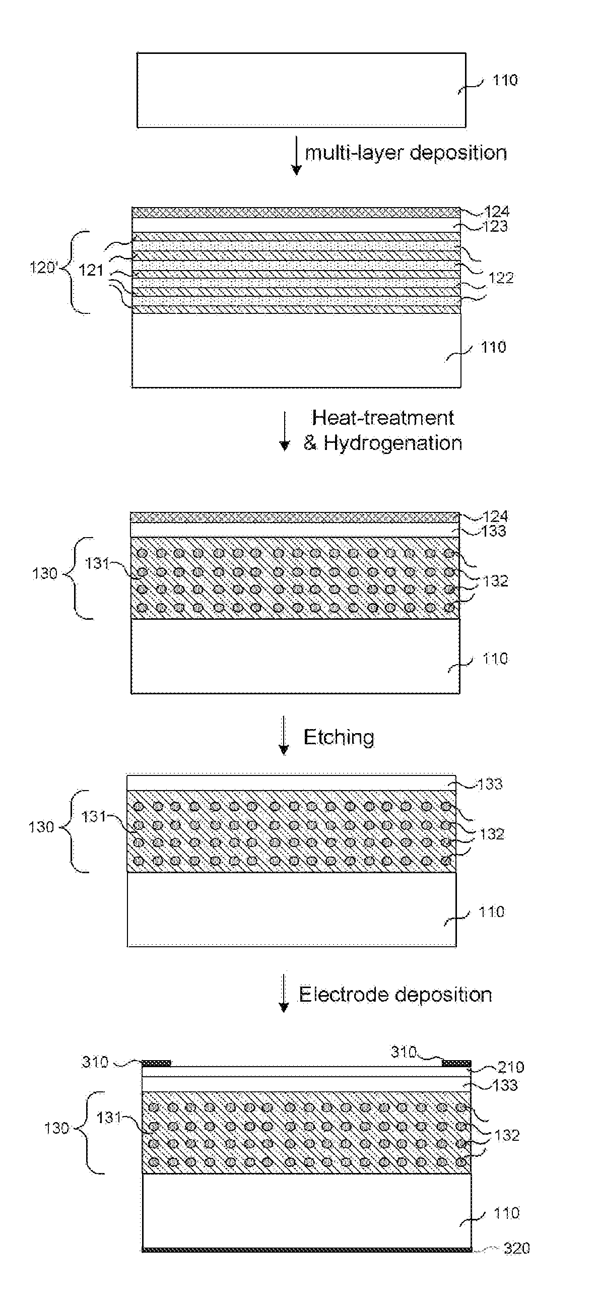
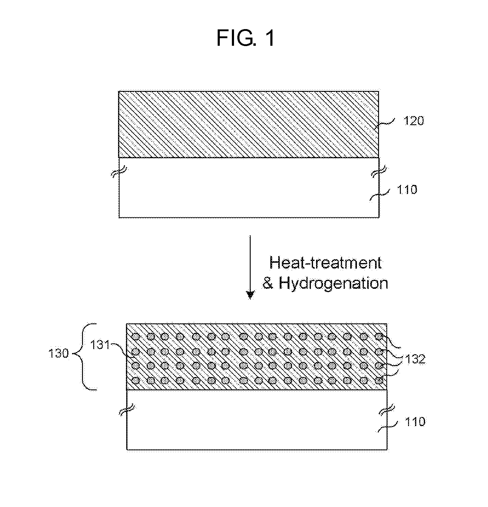
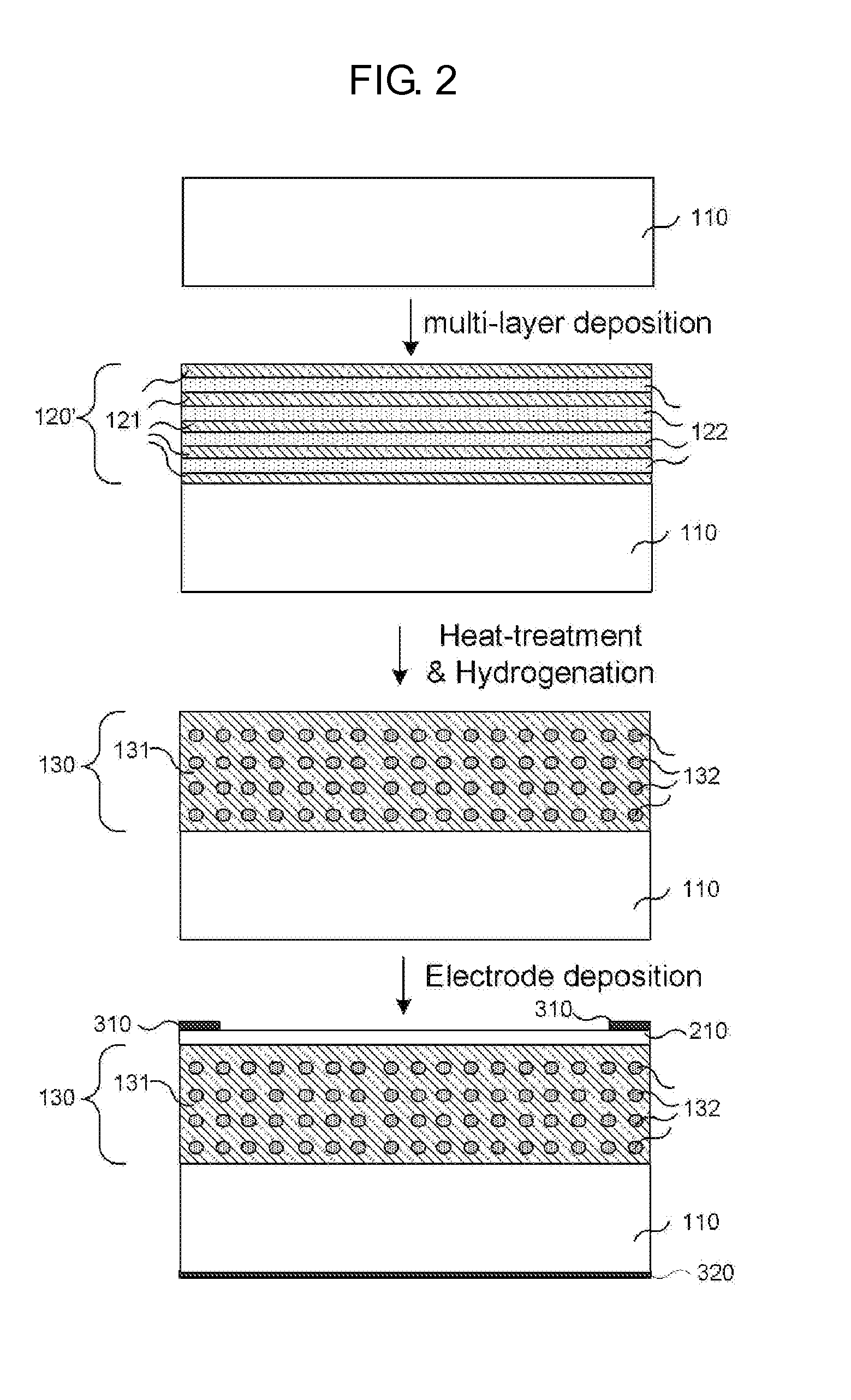
[0026]110: substrate[0027]120: composite stacked multiple layer, 121: matrix layer, 122, 123: semiconductor layer,[0028]130: quantum dot layer, 131: matrix, 132: quantum dot layer,[0029]133: group 4 element layer, 134: surface oxide layer[0030]210: transparent conducting film, 310, 320: electrode

BEST MODE

[0031]Hereinafter, a manufacturing method according to the present invention will be described in detail with reference to the accompanying drawings. The drawings to be provided below are provided by way of example so that the idea of the present invention can be sufficiently transported to those skilled in the art. Therefore, the present invention is not limited to the drawings to be provided below, but may be modified in many different forms. In addition, the drawings to be provided below may be exaggerated in order to clarify the scope of the present invention. Further, like reference numerals denote like elements throughout the specification.

[0032]Here, technical terms and scien...


PUM

PropertyMeasurementUnit
thicknessesaaaaaaaaaa
thicknessaaaaaaaaaa
thicknessaaaaaaaaaa

Abstract

Provided is a manufacturing method of a semiconductor quantum dot-sensitized solar cell. More particularly, the manufacturing method according to the present invention includes: a quantum dot forming step of forming a semiconductor layer containing a group 4 element and InP on a substrate and then performing heat-treatment on the substrate including the semiconductor layer formed thereon to remove indium (In) therefrom, thereby forming an n-type semiconductor quantum dot, which is a group 4 element quantum dot doped with phosphorus (P).

Description

TECHNICAL FIELD[0001]The present invention relates to a quantum dot solar cell and a manufacturing method thereof, and more particularly, to a solar cell in which a having high-concentration P-doped semiconductor quantum dot, and a manufacturing method thereof.BACKGROUND ART[0002]In the case of a photovoltaic device, in order to reduce manufacturing cost and improve efficiency, research into a technology of using various materials except for silicon has been conducted. However, due to characteristics of photovoltaic device using principles of semiconductors, a photovoltaic device made of other materials has low efficiency and a short lifespan due to degradation as compared to a photovoltaic device based on silicon, such that actual market share of the photovoltaic device made of other materials is only about 3%.[0003]In the case of the photovoltaic device based on silicon, single crystalline silicon or polycrystalline silicon is mainly used, and cost of silicon material and wafer is...

Claims


Application Information

Patent Timeline
Patent Type & Authority Applications(United States)
IPC IPC(8): H01L31/18
CPCH01L31/03042H01L31/035218Y02E10/544H01L31/184H01L31/1864H01L31/06Y02P70/50
Inventor KIM, KYUNG JOONGHONG, SEUNG HUIPARK, JAE HEELEE, WOO
Owner KOREA RES INST OF STANDARDS & SCI
Why Eureka
Try Eureka