Method of manufacturing plastic metallized three-dimensional circuit

a three-dimensional circuit and plastic technology, applied in the direction of superimposed coating process, conductive pattern formation, coating, etc., can solve the problems of reducing the selectivity of deposited conducting circuit, requiring rather expensive equipment and manufacturing costs, short circuiting between adjacent electronic elements, etc., to achieve flexibly manufactured, reduce time and cost, and reduce material cost

Inactive Publication Date: 2013-05-23
CHUAN LING HU +1
View PDF4 Cites 19 Cited by
  • Summary
  • Abstract
  • Description
  • Claims
  • Application Information

AI Technical Summary

Benefits of technology

[0019]With the method of manufacturing plastic metallized 3D circuit according to the present invention, the main body can be made of a general plastic material without the need of using a specific material having a doped metal catalyst. Therefore, a wide range of plastic materials can be considered for use to enable reduced material cost. Further, a 3D circuit with complicated circuit pattern can be flexibly manufactured at reduced time and cost without being restricted by mold geometry, machining equipment or complicated circuit structure as in the conventional circuit forming techniques.
[0020]Moreover, the patterned metal circuit is integrally formed on the main body, and there is high bonding strength existed between them to save the procedures of assembling independently manufactured plastic main body and metal conducting plate to one another, and to eliminate the problems of separated metal conducting plate and plastic main body due to assembling error or collision.

Problems solved by technology

That is, the LDS technique requires laser equipment that can provide laser beams of specific wavelengths as well as metallization equipment that can be set to different conditions or control parameters, and therefore, requires rather expensive equipment and manufacturing costs.
Moreover, in using the LDS technique, rising of main body surface temperature would cause removal or breakdown of metal crystal grains on part of the main body surfaces or even cause deposition of metal crystal grains on the main body surfaces at areas not expected for forming the circuit, resulting in reduced selectivity of deposited conducting circuit in the subsequent metallization process and accordingly, the problem of short-circuiting between adjacent electronic elements.
However, large space between circuit paths would often cause another problem of insufficient circuit density.

Method used


Image

  • Method of manufacturing plastic metallized three-dimensional circuit
  • Method of manufacturing plastic metallized three-dimensional circuit
  • Method of manufacturing plastic metallized three-dimensional circuit

Examples


Embodiment Construction

[0028]The present invention will now be described with some preferred embodiments thereof and with reference to the accompanying drawings. It is understood the accompanying drawings are illustrated only for reference and to facilitate easy explanation of the present invention, and not intended to restrict the present invention in any way.

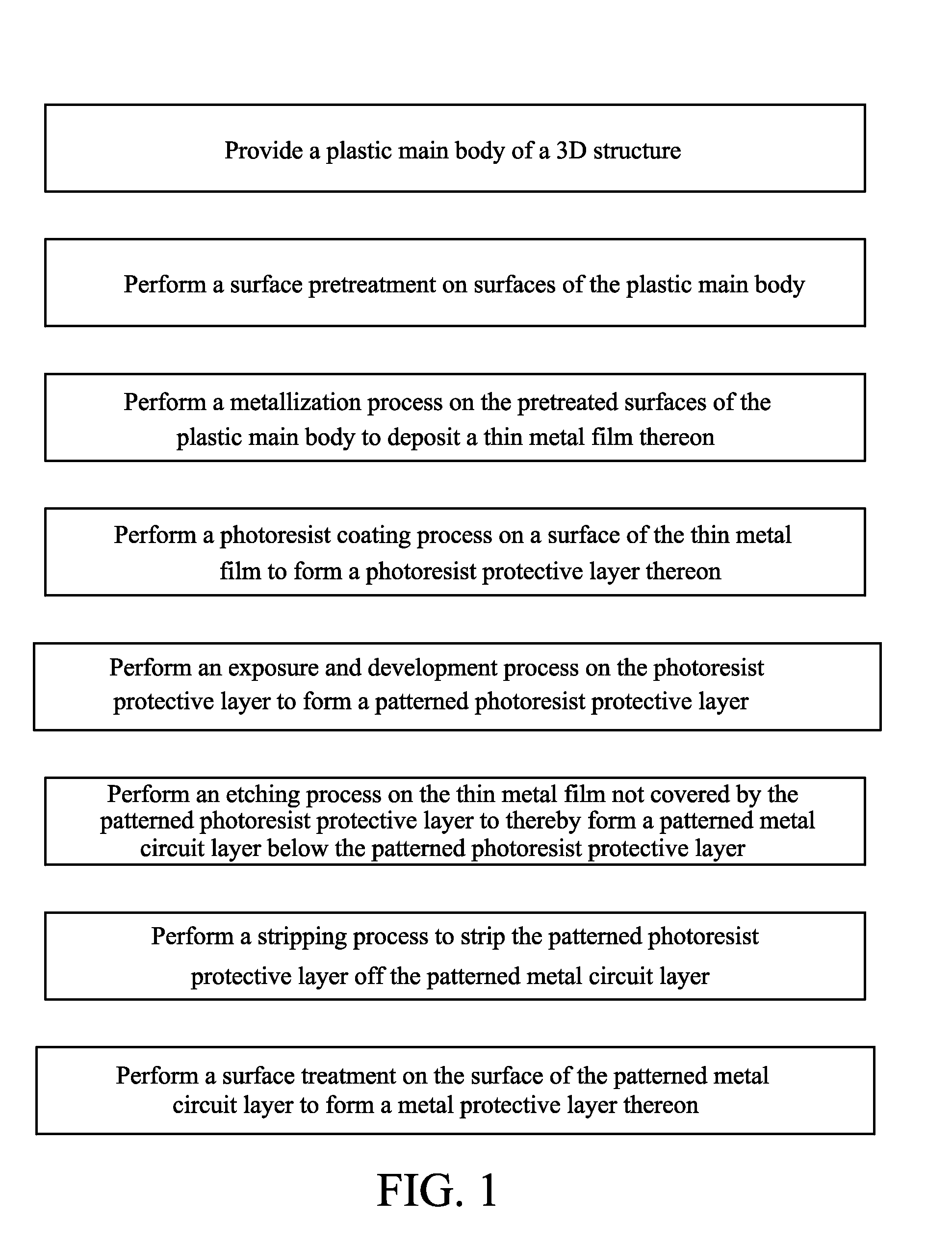
[0029]FIG. 1 is a flowchart showing the steps included in a method of manufacturing plastic metallized three-dimensional (3D) circuit according to a preferred embodiment of the present invention, and FIGS. 2 to 6 are pictorial representations of different steps of the method of the present invention. Please refer to FIG. 1 along with FIGS. 2 to 6.

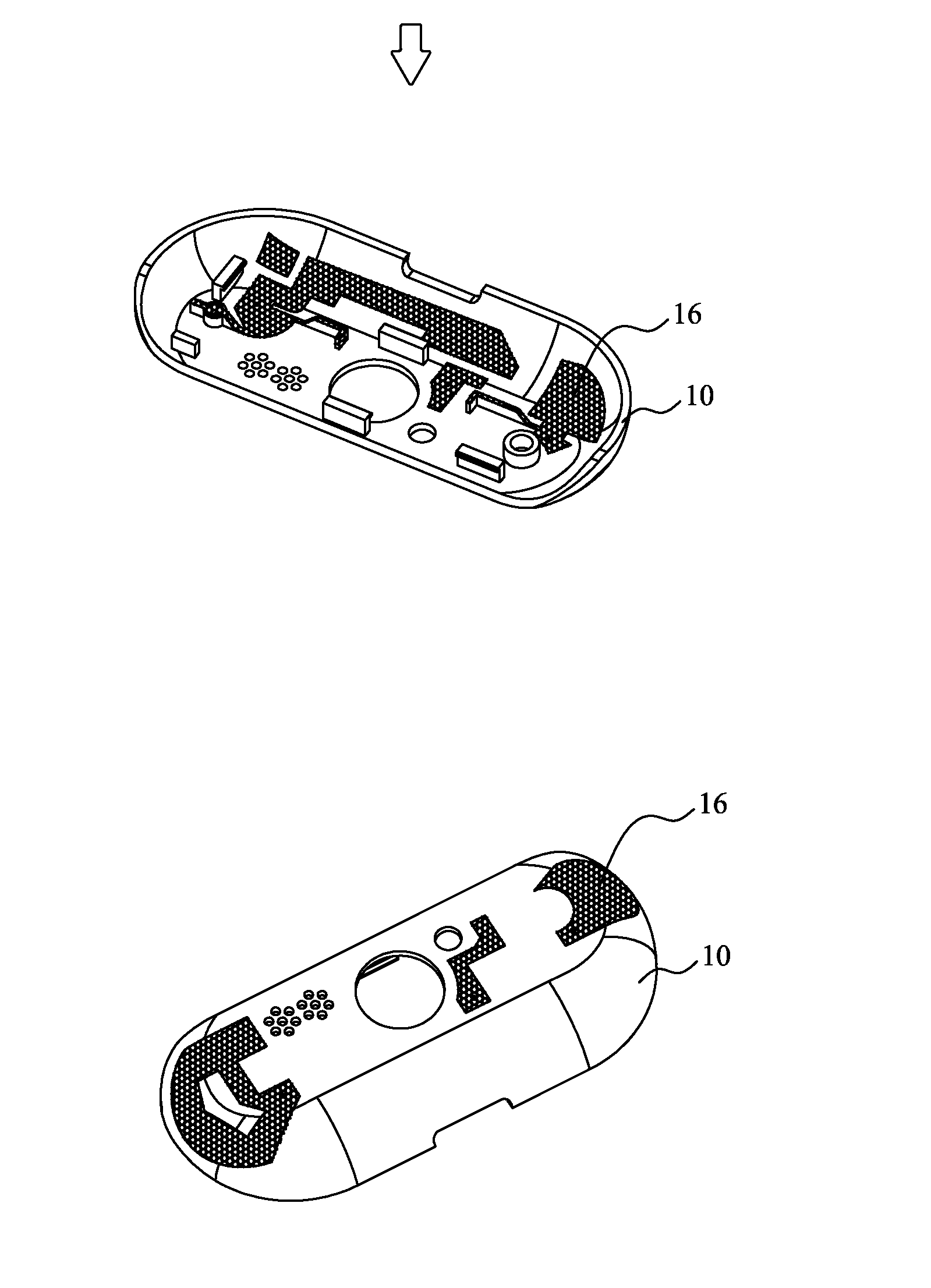
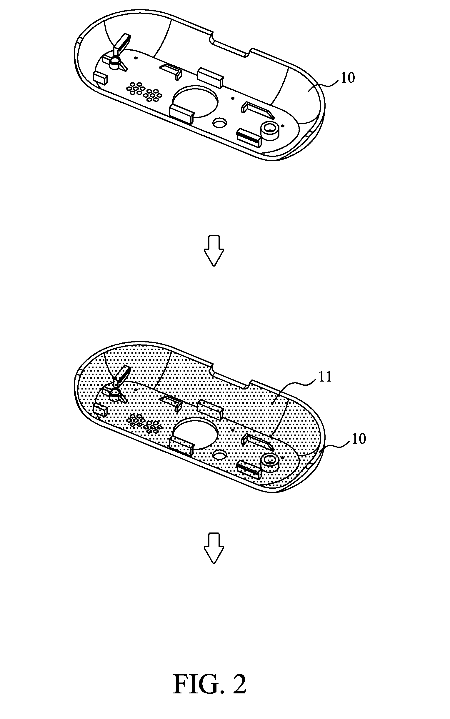
[0030]In a first step of the method, a main body 10 of a 3D structure is provided. The plastic main body 10 is formed by way of injection molding or extrusion molding.

[0031]In a preferred embodiment, the plastic main body 10 is made of a material selected from the group consisting of polyethylene (PE), poly...


PUM

PropertyMeasurementUnit
hydrophilicaaaaaaaaaa
temperatureaaaaaaaaaa
weightaaaaaaaaaa

Abstract

A method of manufacturing plastic metallized 3D circuit includes the steps of providing a 3D plastic main body; performing a surface pretreatment on the plastic main body; performing a metallization process on the plastic main body to deposit a thin metal film thereon; performing a photoresist coating process to form a photoresist protective layer on the thin metal film; performing an exposure and development process on the photoresist protective layer to form a patterned photoresist protective layer; performing an etching process on the exposed thin metal film to form a patterned metal circuit layer; stripping the patterned photoresist protective layer; and performing a surface treatment on the patterned metal circuit layer to form a metal protective layer. With the method, a 3D circuit pattern can be directly formed on a 3D plastic main body without providing additional circuit carrier to thereby meet the requirement for miniaturized and compact electronic devices.

Description

FIELD OF THE INVENTION[0001]The present invention relates to a method of manufacturing plastic metallized three-dimensional (3D) circuit, and more particularly to a method of forming a 3D patterned metal circuit on surfaces of a plastic main body of a 3D structure.BACKGROUND OF THE INVENTION[0002]With the quick development in the wireless communication technological fields, more attention has been drawn to the requirements for signal transmission quality, compactness and low weight of all kinds of electronic communication devices. Generally, antennas for various kinds of mobile video communication products, such as tablet computers and cellular phones, have differently designed main body structures and circuit arrangements corresponding to the appearances and internal structures of the products, in order to satisfy the requirement for miniaturized communication devices.[0003]According to a currently available forming technique, namely, laser direct structuring (LDS), a specific and ...

Claims


Application Information

Patent Timeline
Patent Type & Authority Applications(United States)
IPC IPC(8): C23F17/00
CPCH05K3/06C23C28/021C23F17/00Y10T29/49155H05K1/0284H05K3/182H05K2201/0999H05K3/10
Inventor HU, CHUAN LINGTSAI, CHENG LUNGCHEN, YU WEICHANG, CHEN HAO
Owner CHUAN LING HU
Why Eureka
Try Eureka