Tamper-resistant memory integrated circuit and encryption circuit using same

a technology of integrated circuits and encryption circuits, applied in the field of implementing cryptographic algorithms, can solve the problems of slow processing in these methods, long cryptographic operation compared with the later-described method using dedicated cryptographic hardware, and not only considerably difficult in terms of lsi layout design, so as to achieve high reliability and compatibility. , the effect of high reliability

Inactive Publication Date: 2013-05-23
THE RITSUMEIKAN TRUST
View PDF2 Cites 57 Cited by
  • Summary
  • Abstract
  • Description
  • Claims
  • Application Information

AI Technical Summary

Benefits of technology

[0212]The present invention provides an integrated memory circuit and a cryptographic circuit using the integrated memory circuit, which serve as a highly reliable cryptographic technique with tamper resistance and DPA resistance.
[0213]Further, as described above, by implementing an S-box using a secure memory based on a domino-RSL method as a hardware core, it becomes possible to enable the cryptographic circuit designer to create a DPA-resistant cryptographic circuit without being concerned about the domino-RSL gate. More specifically, the cryptographic circuit layout can be created by designing blocks of the encryption circuit other than the S-box, disposing a secure memory core as a hardware macro during automatic placement and routing, and automatically routing the entire encryption circuit. This eliminates the need for a logic synthesis tool for a domino circuit or a special cell library for a domino-RSL gate. This also eliminates the need to consider the / CLK signal line load required for the domino-RSL gate.
[0214]Moreover, this method also has an advantage in that the same hardware core can be used for the 8 kinds of S-box required for a DES cryptographic circuit by simply changing the data in the secure memory. In the AES cryptographic circuits, which is a new standard regarded as a replacement for conventional DES cryptographic circuits, only the S-box is composed of a nonlinear gate; therefore, the method is easily compatible with the AES cryptographic circuit by using a secure memory with 8-bit input and 8-bit output (capacity: 2 k bits) for an S-box of the AES cryptographic circuit.

Problems solved by technology

As another method for exploiting a cryptographic key, a method in which a cryptographic key is identified by using side channel information such as power consumption of a semiconductor device during execution of a cryptographic algorithm or radiated electromagnetic waves dependent on the power consumption can be a threat.
These cryptographic operations disclosed in Patent Literatures 1 and 2 are generally performed by software using hardware composed of a CPU (central processing unit) and a memory accessible from the CPU, and have a drawback in that the cryptographic operation takes long compared with the later-described method using dedicated cryptographic hardware.
Thus, the processing is slow in these methods.
However, such equalization is not only considerably difficult in terms of LSI layout design, but also causes a practical issue since the implementation area is more than tripled by increasing the number of gates and wiring.
As such, the device consumes constant power regardless of the signal value of the cryptographic device.
However, the system has a problem in that the desired operation result cannot be obtained.
Thus, it is difficult to equip an LSI with an asynchronous signal circuit capable of accurate timing control.
Therefore, this method has a feature in that it is not necessary to control asynchronous timing of / en signals, which is difficult to implement in the RSL method.

Method used


Image

  • Tamper-resistant memory integrated circuit and encryption circuit using same
  • Tamper-resistant memory integrated circuit and encryption circuit using same
  • Tamper-resistant memory integrated circuit and encryption circuit using same

Examples


Embodiment Construction

[0244]Hereinafter, an embodiment according to the present invention will be described based on the accompanying drawings.

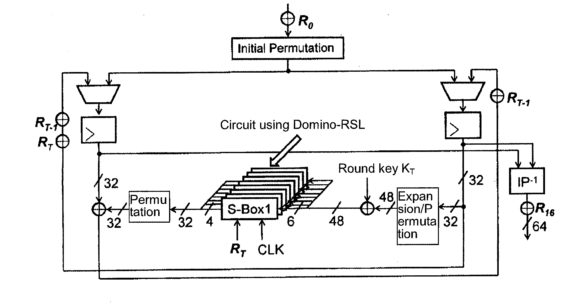
[0245]FIG. 8 shows a function block diagram of a tamper-resistant integrated memory circuit (secure memory) according to the embodiment of the present invention. This secure memory is composed of a memory array, a row decoder composed of an address predecoder and a word line driver, a column decoder, a sense amplifier, and an input / output driver. The secure memory receives a clock CLK, address data A, and a control signal / Write from the outside, and performs writing / reading of data on a corresponding memory cell in the memory array. The secure memory is different from a general memory in that a random number R is supplied into the secure memory from an external random-number generator (not shown). The address A is an input, and data D is input / output. If the secure memory is used as an S-box of a DES cryptographic circuit, the address A is a 6-bit input, and the ...


PUM


Abstract

The present invention provides an integrated memory circuit applicable to an S-box of a cryptographic circuit, the integrated memory circuit having a row decoder, a column decoder, and a sense amplifier composed of a domino-RSL circuit, wherein data reading and data writing from / to memory cells of a memory cell array are performed via two complementary bit lines, and the transition probability of a signal line is equalized by input of random-number data supplied from a random-number generating circuit using an arbiter circuit.

Description

TECHNICAL FIELD[0001]The present invention relates to a semiconductor device for implementing a cryptographic algorithm. In particular, the present invention relates to a tamper-resistant integrated memory circuit equipped with a countermeasure against attacks for exploiting secret information (mainly cryptographic keys) processed by a semiconductor device, by using side channel information such as power consumption of the semiconductor device or radiated electromagnetic waves dependent on the power consumption. The present invention also relates to a cryptographic circuit using the tamper-resistant integrated memory circuit.BACKGROUND ART[0002]In recent years, a system (e.g., an IC card) for storing financial information or personal information by using an LSI has become widely popular, and the importance of ensuring the reliability and security of such a security LSI is significantly increasing. In the security LSI, confidential information is protected by using a cryptographic ci...

Claims


Application Information

Patent Timeline
Patent Type & Authority Applications(United States)
IPC IPC(8): G11C8/08H04L9/00G11C7/12H04L9/28G11C8/00G11C7/00G06F7/58
CPCG11C7/24H04L9/003H04L9/0618H04L9/28G06F7/584G11C7/12G11C8/08H04L2209/127
Inventor FUJINO, TAKESHI
Owner THE RITSUMEIKAN TRUST
Why Eureka
Try Eureka