Apparatus and method of direct writing with photons beyond the diffraction limit

a technology of photons and diffraction limits, applied in the field of lithography, can solve the problems of euv lithography systems not being commercially viable, the inability to keep reducing the fundamental material limitations of the minimum geometry of ic chips, etc., and achieves the effects of low contrast, low cost, and high contrast ratio

Active Publication Date: 2013-05-23
PERIODIC STRUCTURES
View PDF4 Cites 28 Cited by
  • Summary
  • Abstract
  • Description
  • Claims
  • Application Information

AI Technical Summary

Benefits of technology

[0014]The single broadband objective lens images all 2,000,000 pixels simultaneously rather than requiring a separate lens for each pixel. A refractive lens efficiently gathers all the light from an image-transducer pixel and concentrates it on a small region on the image. This feature is not available with zone plates that have very small fields, very restricted spectral ranges, and efficiencies of about 40%, assuming they are made of alternating rings of transparent and opaque materials.
[0075]Another aspect of the disclosure is a method that employs the system as described above, wherein the four active pixels closest to a given pixel have a phase shift at the exposing wavelength relative to the given pixel and wherein the phase shift is optimized to minimize the influence of the surrounding pixels on the exposure created by the given pixel.

Problems solved by technology

However, the ability to keep reducing the minimum geometry of IC chips is reaching fundamental material limitations.
Beyond 193 nm there are no glass materials suitable for use as the lenses, and the transmission of such short-wavelength light through air is problematic.
While serious effort is presently being directed toward using extreme-ultra-violet (EUV) wavelengths in the X-ray region at 13.5 nm in combination with mirror systems, it is not yet clear whether EUV lithography systems will be commercially viable.
Conventional mask-based optical lithography is limited mainly by the diffraction limit of the projection imaging process.
This is not possible with a zone-plate-array-based system.
Any appreciable inhibition light in the center of the dark spot (black hole) between the orthogonal fringes can result in an underexposed or a missing image.
Even if the illumination across the grating is not uniform, this non-uniformity will have little if any effect on the image contrast, because the grating is imaged directly on the substrate.
This rigor is not available with zone plates, with which there is no way of eliminating other possible orders.
It may prove very difficult to achieve the desired image contrast, especially with a dichroic zone plate.
The undetected failure of a single pixel in the image transducer, of a single laser diode in the inhibition or exposure illumination paths or of one of the fringe shifters could lead to the scrapping of millions of dollars of product wafers.
An occasional failure of any of these components cannot be ruled out, but with the system described, the failure of any of these components can be detected quickly and easily.
Previous hardware concepts did not meet the throughput threshold that would have made them viable for high-volume production and therefore did not attract the funding necessary for a supportive resist-and-image-transducer infrastructure.

Method used


Image

  • Apparatus and method of direct writing with photons beyond the diffraction limit
  • Apparatus and method of direct writing with photons beyond the diffraction limit
  • Apparatus and method of direct writing with photons beyond the diffraction limit

Examples


example

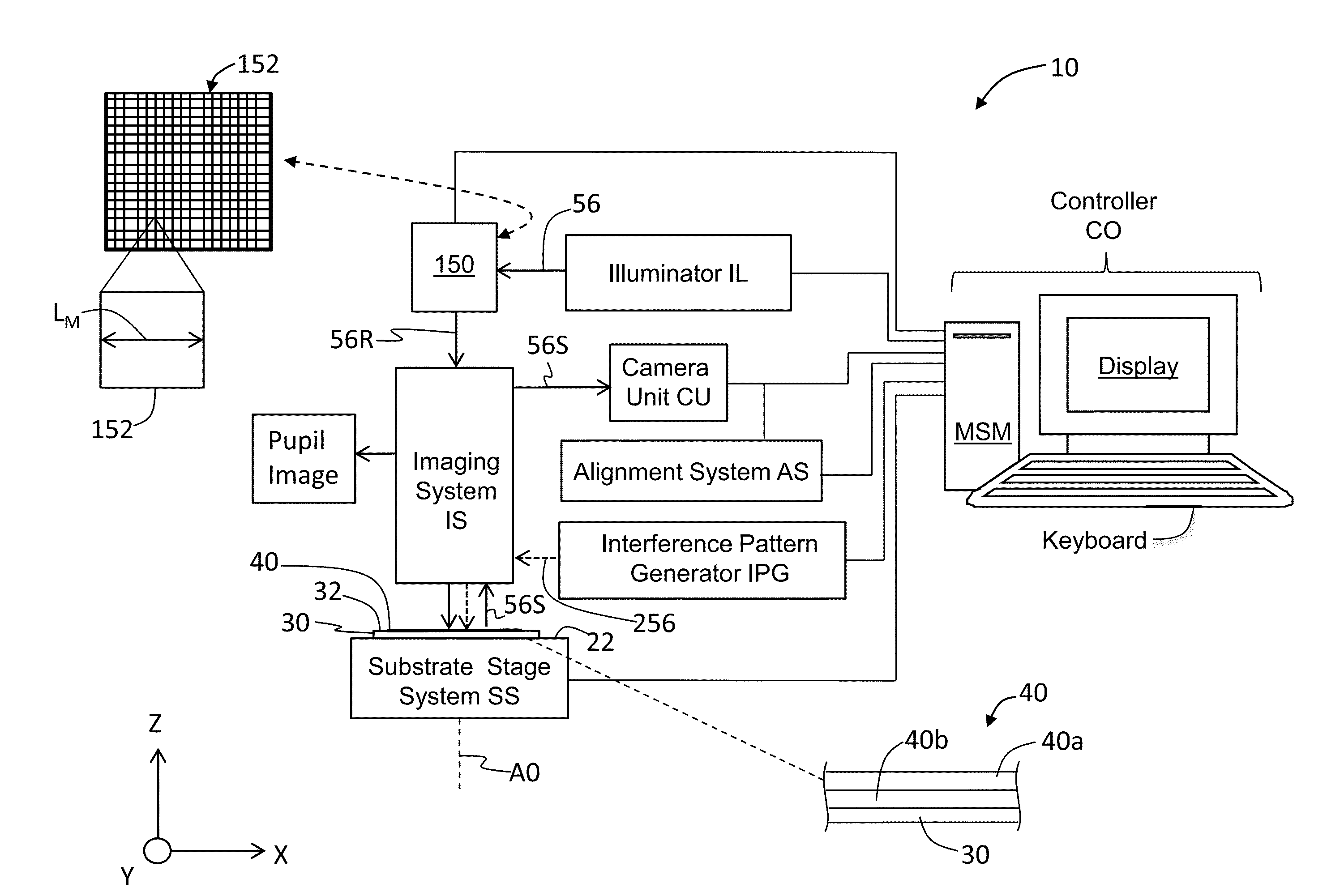
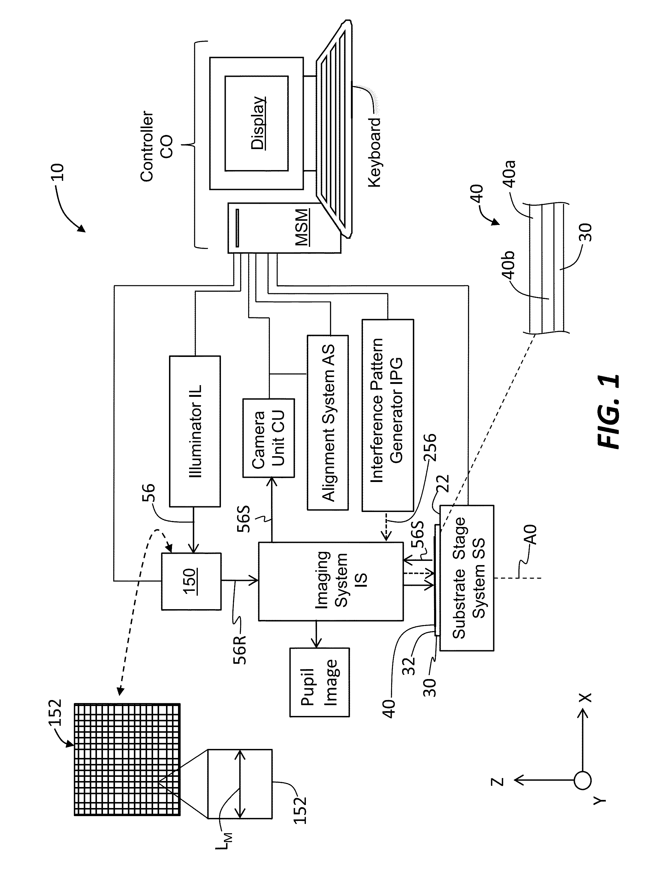
[0221]An example apparatus 10 has a DMD-based image transducer 150 with micro-mirrors 152 as pixels having a center-to-center spacing SC of 10.8 microns, an inhibition wavelength λ2=532 nm, and a numerical aperture NA=0.9 for objective lens 170. The spacing SF of fringes 160X and 160Y at substrate 30 is given by:

SF=λ / 2NA=(0.532 microns) / (2×0.9)=0.2956 microns

The inhibition fringe spacing SF is equal to the DMD pixel size L′M=LM / M, where M is the de-magnification of objective lens 170. Thus,

L′M=(10.8 microns) / M=0.2956 microns

The magnification ratio M is therefore:

M=10.8 / 0.2956=36.541

Assuming the resolution R is 1 / 20 of the substrate pixel size, which is commensurate with experimental results, the minimum feature size LP that can be imaged is given by:

LP=(0.2956 microns) / 20=14.8 nm.
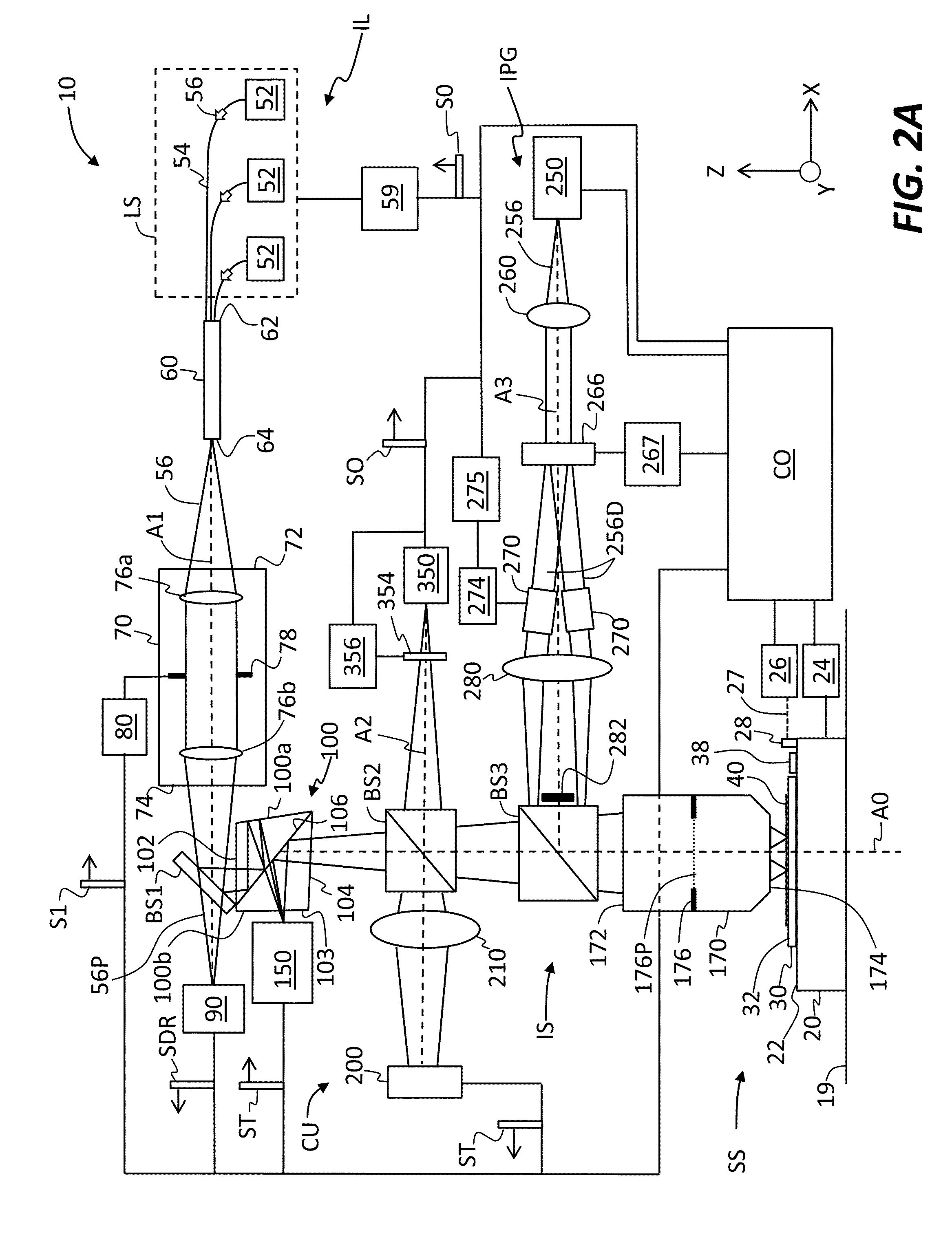
Optical Modelling

[0222]FIG. 3 shows a small segment of the crossed-fringe interference image 158 as formed at substrate 30 or in photoresist 40 deposited thereupon. The regular pattern of dark spots 300D is...


PUM

PropertyMeasurementUnit
inhibition wavelengthaaaaaaaaaa
sizeaaaaaaaaaa

Abstract

Direct-write lithography apparatus and methods are disclosed in which a transducer image and an image of crossed interference fringe patterns are superimposed on a photoresist layer supported by a substrate. The transducer image has an exposure wavelength and contains bright spots, each corresponding to an activated pixel. The interference image has an inhibition wavelength and contains dark spots where the null points in the crossed interference fringes coincide. The dark spots are aligned with and trim the peripheries of the corresponding bright spot to form sub-resolution photoresist pixels having a size smaller than would be formed in the absence of the dark spots.

Description

CLAIM OF PRIORITY[0001]This application claims priority under 35 U.S.C. §119(e) from U.S. Provisional Application Ser. No. 61 / 561,545, filed on Nov. 18, 2011, which application is incorporated by reference herein.STATEMENT OF GOVERNMENT RIGHTS[0002]This disclosure was made with government support under Contract #N66001-10-C-406, awarded by DARPA and managed by SPAWAR Systems Center Pacific. The government therefore has certain rights in the disclosure.FIELD[0003]The present disclosure relates to lithography, and in particular to super-resolution lithography apparatus and methods that utilize direct writing with photons.BACKGROUND ART[0004]The semiconductor device manufacturing industry has relied on optical lithography techniques since the 1960s to produce ever denser and more powerful integrated circuit (IC) chips. However, the ability to keep reducing the minimum geometry of IC chips is reaching fundamental material limitations. The continued use of optical lithography has been en...

Claims


Application Information

Patent Timeline
Patent Type & Authority Applications(United States)
IPC IPC(8): G03B27/52G03F7/20
CPCG03B27/522G03F7/70383G03F7/2051
Inventor MARKLE, DAVID A.HENDEL, RUDOLF H.PETERSEN, JOHN S.
Owner PERIODIC STRUCTURES
Why Eureka
Try Eureka