Semiconductor Field-Effect Transistor Structure and Method for Manufacturing the Same

a semiconductor and field-effect transistor technology, applied in the direction of semiconductor devices, basic electric elements, electrical appliances, etc., can solve the problems of high manufacturing cost, many shortcomings of soi finfets, and the problem of severe challenges facing the planar bulk silicon cmos structure device, so as to reduce manufacturing cost, easy to form local soi structures, and reduce manufacturing costs

Active Publication Date: 2013-05-30
INST OF MICROELECTRONICS CHINESE ACAD OF SCI
View PDF10 Cites 8 Cited by
  • Summary
  • Abstract
  • Description
  • Claims
  • Application Information

AI Technical Summary

Benefits of technology

[0019]As shown in foregoing technical solution, the present invention brings forth following favorable effects.
[0020]1. The semiconductor FET structure and the manufacturing method thereof provided by the present invention make it possible to manufacture FinFET devices on bulk silicon substrates, which lowers manufacturing cost, and overcomes self-heating effects and floating body effects existing in SOI FinFET devices, and reduce manufacturing cost as well.
[0021]2. The semiconductor FET structure and the manufacturing method thereof provided by the present invention make it easy to form local SOI structures on bulk silicon substrates and easy to manufacture fin structures isolated from substrates, so as to considerably alleviate difficulty for manufacturing FinFETs.
[0022]3. According to the semiconductor FET structure and the manufacturing method thereof provided by the present invention, the manufacturing processes are simple to implement, integration is quite easy, and compatibility with planar CMOS process is very good.

Problems solved by technology

As the integrated circuit industry has been developed according to Moore's law, feature sizes of CMOS devices are continuously scaled down, planar bulk silicon CMOS structure devices are now facing severe challenges.
However, SOI FinFETs still suffer from many shortcomings like high manufacturing cost, poor heat dissipation, floating body effects and poor compatibility with CMOS process.
The floating body effects would cause lots of problems like reduction in gain of devices, noise overshoot, instable operation of devices, and decrease in breakdown voltage of source and drain.
Besides, performance of heat dissipation would be lowered in SOI FinFET devices because of the existence of BOX, which consequently causes self-heating effect; accordingly, drift mobility, threshold voltage, impact ionization, leakage current, sub-threshold slope and the like would be affected by temperature.

Method used


Image

  • Semiconductor Field-Effect Transistor Structure and Method for Manufacturing the Same
  • Semiconductor Field-Effect Transistor Structure and Method for Manufacturing the Same
  • Semiconductor Field-Effect Transistor Structure and Method for Manufacturing the Same

Examples


Embodiment Construction

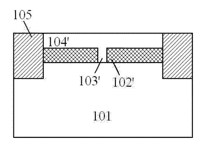
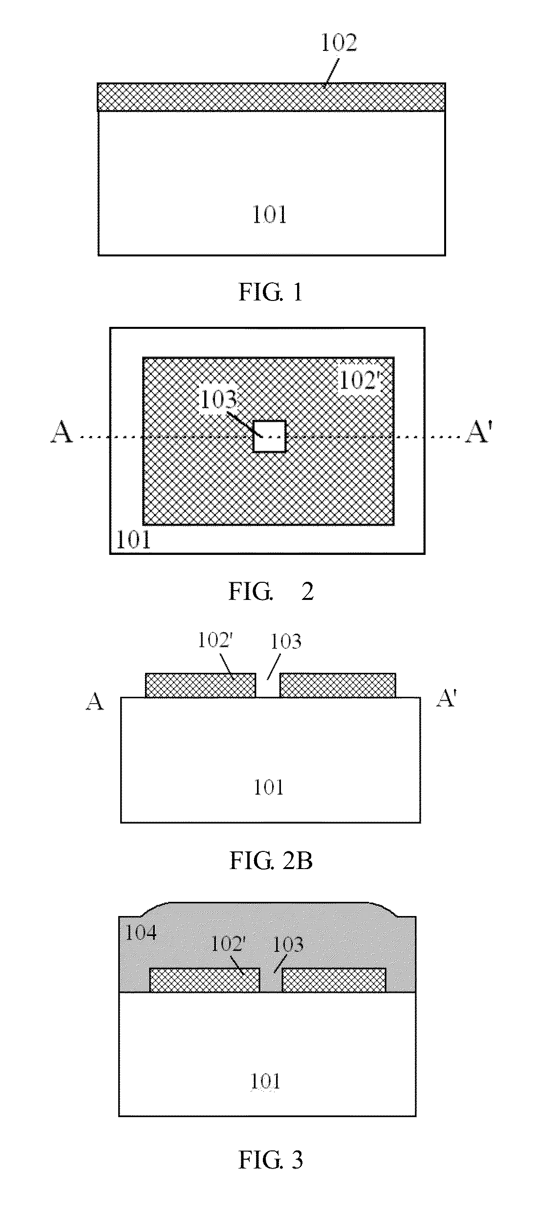
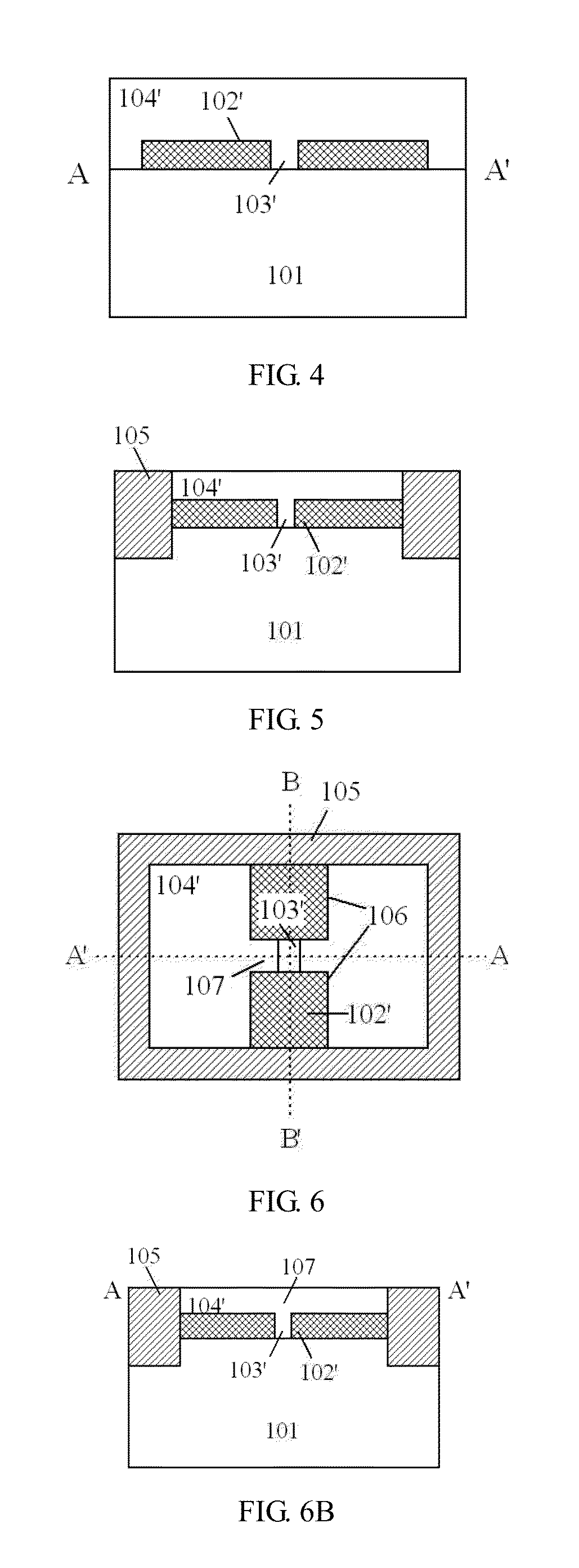
[0027]Here below, the present invention is described in detail in view of embodiments illustrated in the accompanying drawings. However, it should be understood that the description is exemplary but not to limit the scope of the present invention. Besides, description of conventional components, processing technology and crafts are omitted in the following text in order not to unnecessarily obscure the present invention.

[0028]Diagrams of layer structures according to embodiments of the present invention are illustrated in accompanying drawings, whereas the diagrams are not drawn to scale, wherein some details are enlarged while certain details might be omitted for purpose of clarity. Various regions, shapes of layers, and relative sizes, positional relationship thereof shown in the drawings are illustrative only, slight difference might occur because of permitted manufacturing difference or technical limits in practice; besides, a person of ordinary skill in the art can otherwise de...


PUM


Abstract

The present application discloses a semiconductor Field-Effect Transistor (FET) structure and a method for manufacturing the same, wherein the method comprises: forming a semiconductor substrate comprising an SOI structure having a body-contact hole; forming a fin on the SOI structure of the semiconductor substrate; forming a gate stack structure on top and side faces of the fin; forming source / drain structures in the fin on both sides of the gate stack structure; and performing metallization. The present invention makes use of traditional quasi-planar based top-down processes, thus the manufacturing process thereof becomes simple to implement; the present invention exhibits good compatibility with CMOS planar process and can be easily integrated; the present invention also is favorable for suppressing short channel effects desirably, and boosts MOSFETs to develop towards a trend of downscaling size.

Description

[0001]The present application claims priority to Chinese Patent application No. 201110212835.X, filed on Jul. 27, 2011, entitled “SEMICONDUCTOR FIELD EFFECT TRANSISTOR STRUCTURE AND METHOD FOR MANUFACTURING THE SAME”, which is incorporated herein by reference in its entirety.FIELD OF THE INVENTION[0002]The present invention relates to semiconductor manufacturing field, particularity, to a method for manufacturing Fin Field-Effect Transistors (FinFETs).BACKGROUND OF THE INVENTION[0003]As the integrated circuit industry has been developed according to Moore's law, feature sizes of CMOS devices are continuously scaled down, planar bulk silicon CMOS structure devices are now facing severe challenges. In order to overcome these problems, various new device structures have been invented; among these new device structures, Fin Field-Effect Transistor (FinFET) has been regarded as one of the new structure devices that will most probably replace planar bulk silicon CMOS devices, and therefor...

Claims


Application Information

Patent Timeline
Patent Type & Authority Applications(United States)
IPC IPC(8): H01L29/66H01L29/78
CPCH01L21/845H01L27/1211H01L29/7851H01L29/785H01L29/66795
Inventor ZHOU, HUAJIEXU, QIUXIA
Owner INST OF MICROELECTRONICS CHINESE ACAD OF SCI
Why Eureka
Try Eureka