Method for forming oxide semiconductor film and method for manufacturing semiconductor device

a semiconductor film and oxide technology, applied in the direction of semiconductor devices, basic electric elements, electrical equipment, etc., can solve the problems of unsatisfactory filling of oxygen vacancies and generation of charges, and achieve the effect of shortening the distance between oxygen ions traveling to the oxide semiconductor film formed over the base insulating film, favorable electrical characteristics, and unfavorable electrical characteristics

Inactive Publication Date: 2013-05-30
SEMICON ENERGY LAB CO LTD
View PDF8 Cites 21 Cited by
  • Summary
  • Abstract
  • Description
  • Claims
  • Application Information

AI Technical Summary

Benefits of technology

[0029]In the above embodiment, the sacrifice film can be formed using a material that is the same as or different from that for the film formed under the sacrifice film. By forming the sacrifice film with the use of a material that is different from that for the film formed under the sacrifice film, the sacrifice film can be easily removed by utilizing etching selectivity at the removal of the sacrifice film. By forming the sacrifice film with the use of the same material as the film formed under the sacrifice film, the time taken to form the film of one embodiment of the present invention can be shortened, and impurities which might be attached to the film formed under the sacrifice film in the case where the sacrifice film is formed using a material that is different from that for the film formed under the sacrifice film can be reduced.
[0034]Further, when the local maximum of the oxygen ion concentration distribution is located in the vicinity of the surface of the base insulating film, the distance which the oxygen ion travels to the oxide semiconductor film formed over the base insulating film can be shortened; thus, oxygen vacancies in the oxide semiconductor film can be effectively filled. Accordingly, a transistor having favorable electrical characteristics can be manufactured.
[0035]When oxygen ions are injected into an injection target such as an oxide semiconductor film or an insulating film by an ion implantation method or an ion doping method, not only the injected oxygen ions but also impurities attached to the injection target are put into the injection target owing to a knock-on effect. If a transistor is manufactured using such an injection target including impurities, the transistor might have unfavorable electrical characteristics. In contrast, by forming a sacrifice film, and then injecting oxygen ions and removing the sacrifice film as in one embodiment of the present invention, impurities included in an injection target can be reduced, and thus, a transistor having favorable electrical characteristics can be manufactured.
[0036]According to one embodiment of the present invention, a method for forming an oxide semiconductor film into which oxygen ions are uniformly injected can be provided. Furthermore, according to one embodiment of the present invention, a method for manufacturing a semiconductor device having favorable electrical characteristics with the use of the oxide semiconductor film can be provided.

Problems solved by technology

However, in an oxide semiconductor, charge is generated owing to an oxygen vacancy caused therein.
Consequently, the lowering of the acceleration voltage for oxygen ion injection leads to a non-uniform concentration of the injected oxygen ions in the depth direction of the oxide semiconductor, and thus, oxygen vacancies might not be sufficiently filled.

Method used


Image

  • Method for forming oxide semiconductor film and method for manufacturing semiconductor device
  • Method for forming oxide semiconductor film and method for manufacturing semiconductor device
  • Method for forming oxide semiconductor film and method for manufacturing semiconductor device

Examples


embodiment 1

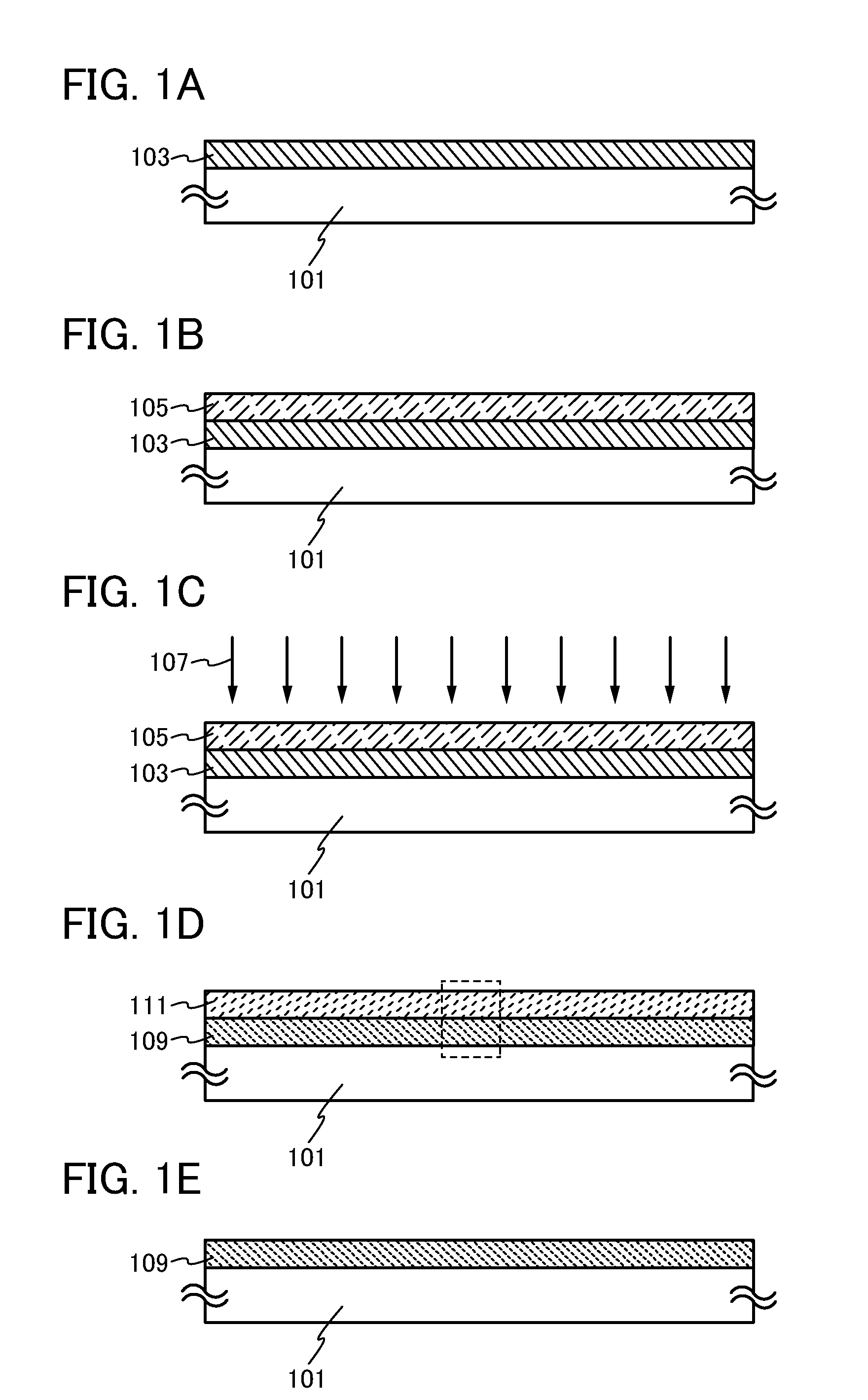
[0060]In this embodiment, a method for forming an oxide semiconductor film in which oxygen is contained uniformly in the depth direction of the oxide semiconductor film is described with reference to FIGS. 1A to 1E and FIG. 16A. FIGS. 1A to 1E are schematic cross-sectional views illustrating a method for forming an oxide semiconductor film, which is one embodiment of the present invention.

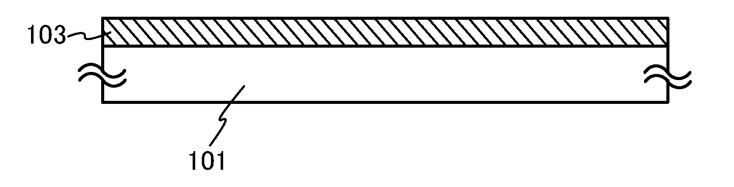
[0061]First, an oxide semiconductor film 103 is formed over a substrate 101 (see FIG. 1A). The oxide semiconductor film 103 may be formed using any of metal oxide materials (oxide semiconductor materials) given below by a chemical vapor deposition (CVD) method, a sputtering method, a molecular beam epitaxy (MBE) method, or a pulsed laser deposition (PLD) method, and is preferably formed by a sputtering method.

[0062]The oxide semiconductor film 103 may have an amorphous structure or a crystalline structure.

[0063]For the oxide semiconductor film 103, a metal oxide material containing at least indium ...

embodiment 2

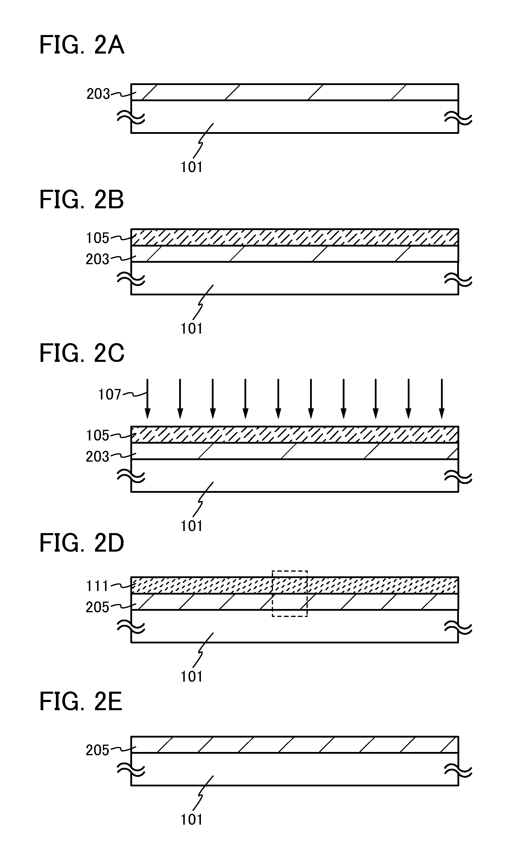
[0088]In this embodiment, a method for forming an insulating film in which oxygen is contained uniformly in the depth direction of the insulating film is described with reference to FIGS. 2A to 2E and FIG. 16B. FIGS. 2A to 2E are schematic cross-sectional views illustrating a method for forming an insulating film, which is one embodiment of the present invention.

[0089]First, an insulating film 203 is formed over the substrate 101 (see FIG. 2A). The insulating film 203 may be formed by a CVD method, a sputtering method, an MBE method, or a PLD method.

[0090]There is no particular limitation on the insulating film 203 as long as it is an insulator. For example, an oxide insulating film of silicon oxide or the like, a nitride insulating film of silicon nitride or the like, an oxynitride insulating film of silicon oxynitride or the like, or a nitride oxide insulating film of silicon nitride oxide or the like can be used.

[0091]Note that silicon oxynitride refers to a substance that contai...

embodiment 3

[0112]In this embodiment, a method for manufacturing a semiconductor device with the use of the method for forming an oxide semiconductor film described in Embodiment 1 is described. Note that a transistor using an oxide semiconductor is described as an example of the semiconductor device in this embodiment. In addition, the method for forming an oxide semiconductor film described in Embodiment 1 can be applied to the manufacture of transistors having a variety of structures, such as a top-gate transistor, a bottom-gate transistor, and a dual-gate transistor; a top-gate transistor is described here as an example.

[0113]FIGS. 3A to 3D are schematic cross-sectional views illustrating a method for manufacturing a transistor using an oxide semiconductor in this embodiment.

[0114]First, the substrate 101 is prepared. Although there is no particular limitation on the substrate 101, it is preferable that the substrate 101 have an insulating surface and at least heat resistance high enough to...


PUM


Abstract

An oxide semiconductor film is formed over a substrate. A sacrifice film is formed to such a thickness that the local maximum of the concentration distribution of an injected substance injected into the oxide semiconductor film in the depth direction of the oxide semiconductor film is located in a region from an interface between the substrate and the oxide semiconductor film to a surface of the oxide semiconductor film. Oxygen ions are injected as the injected substance into the oxide semiconductor film through the sacrifice film at such an acceleration voltage that the local maximum of the concentration distribution of the injected substance in the depth direction of the oxide semiconductor film is located in the region, and then the sacrifice film is removed. Further, a semiconductor device is manufactured using the oxide semiconductor film.

Description

BACKGROUND OF THE INVENTION[0001]1. Field of the Invention[0002]The present invention relates to a method for forming an oxide semiconductor film or an insulating film, and to a method for manufacturing a semiconductor device with the use of the oxide semiconductor film or the insulating film.[0003]Note that a semiconductor device in this specification refers to general devices which can function by utilizing semiconductor characteristics; for example, a semiconductor element such as a transistor, a semiconductor circuit including a semiconductor element, an electro-optical device such as a display device, and an electronic device are all semiconductor devices.[0004]2. Description of the Related Art[0005]Transistors used for most flat panel displays typified by a liquid crystal display device and a light-emitting display device are formed using silicon semiconductors such as amorphous silicon, single crystal silicon, and polycrystalline silicon provided over glass substrates. Furthe...

Claims


Application Information

Patent Timeline
Patent Type & Authority Applications(United States)
IPC IPC(8): H01L29/66H01L21/265
CPCH01L29/66477H01L29/7869H01L29/66969H01L21/265H01L21/02565
Inventor ITO, DAIGOSATO, YUICHINODA, KOSEI
Owner SEMICON ENERGY LAB CO LTD
Why Eureka
Try Eureka