Dram cache with tags and data jointly stored in physical rows

a cache and physical row technology, applied in the field of computing systems, can solve the problems of limiting potential benefits, increasing the delay of interconnection per unit length, and high electrical impedance between individual chips, so as to reduce latency and power consumption

Active Publication Date: 2013-05-30
ADVANCED MICRO DEVICES INC
View PDF9 Cites 98 Cited by
  • Summary
  • Abstract
  • Description
  • Claims
  • Application Information

AI Technical Summary

Benefits of technology

[0012]In various embodiments, the 3D DRAM may store both a tag array and a data array. Each row of the multiple rows in the memory array banks of the 3D DRAM may store one or more cache tags and one or more corresponding cache lines indicated by the one or more cache tags. In response to receiving a memory request from the processing unit, the 3D DRAM may perform a memory access...

Problems solved by technology

However, design issues still arise with modern techniques in processing and integrated circuit design that may limit potential benefits.
One issue is that interconnect delays continue to increase per unit length in successive generations of two-dimensional planar layout chips.
Also, high electrical impedance between individual chips increases latency.
In addition, signals that traverse off-chip to another die may significantly increase power consumption for these signals (e.g., by 10 to 100 times) due to the increased parasitic capacitance on these longer signal routes.
Another design issue is that most software applications that access a lot of data are typically memory bound in that computation time is generally determined by memory bandwidth.
A memory access latency for an off-chip dynamic random access memory (DRAM) may be hundreds to over a thousand clock cycles, and an increased number of cores in a proce...

Method used


Image

  • Dram cache with tags and data jointly stored in physical rows
  • Dram cache with tags and data jointly stored in physical rows
  • Dram cache with tags and data jointly stored in physical rows

Examples


Embodiment Construction

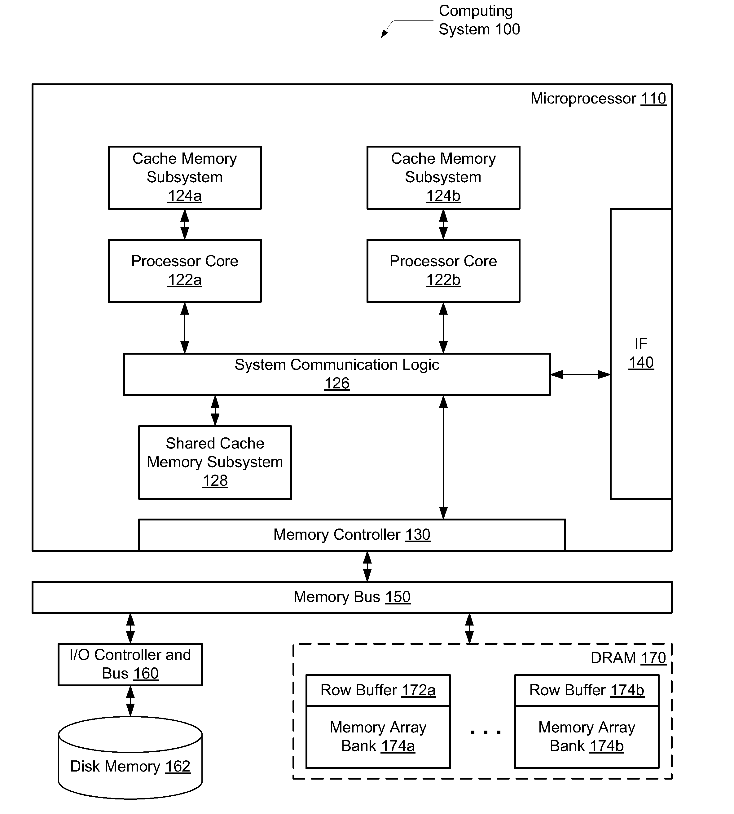
[0010]Systems and methods for efficient cache data access in a large row-based memory of a computing system are contemplated.

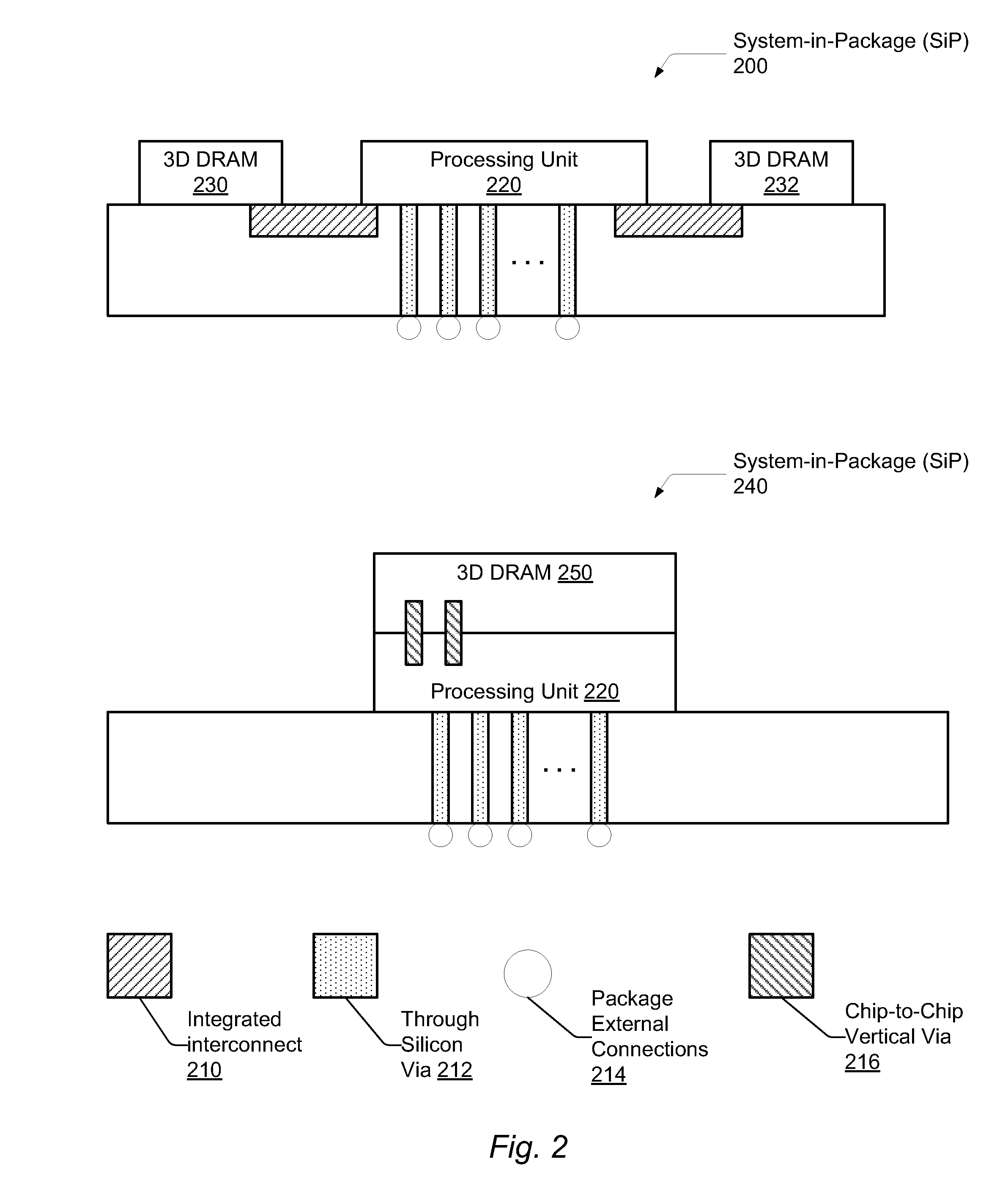
[0011]In one embodiment, a computing system includes a processing unit and an integrated dynamic random access memory (DRAM). Examples of the processing unit include a general-purpose microprocessor, a graphics processing unit (GPU), an accelerated processing unit (APU), and so forth. The integrated DRAM may be a three-dimensional (3D) DRAM and may be included in a System-in-Package (SiP) with the processing unit. The processing unit may utilize the 3D DRAM as a cache.

[0012]In various embodiments, the 3D DRAM may store both a tag array and a data array. Each row of the multiple rows in the memory array banks of the 3D DRAM may store one or more cache tags and one or more corresponding cache lines indicated by the one or more cache tags. In response to receiving a memory request from the processing unit, the 3D DRAM may perform a memory access according to the ...


PUM


Abstract

A system and method for efficient cache data access in a large row-based memory of a computing system. A computing system includes a processing unit and an integrated three-dimensional (3D) dynamic random access memory (DRAM). The processing unit uses the 3D DRAM as a cache. Each row of the multiple rows in the memory array banks of the 3D DRAM stores at least multiple cache tags and multiple corresponding cache lines indicated by the multiple cache tags. In response to receiving a memory request from the processing unit, the 3D DRAM performs a memory access according to the received memory request on a given cache line indicated by a cache tag within the received memory request. Rather than utilizing multiple DRAM transactions, a single, complex DRAM transaction may be used to reduce latency and power consumption.

Description

BACKGROUND OF THE INVENTION[0001]1. Field of the Invention[0002]This invention relates to computing systems, and more particularly, to efficient cache data access in a large row-based memory of a computing system.[0003]2. Description of the Relevant Art[0004]As both semiconductor manufacturing processes advance and on-die geometric dimensions reduce, semiconductor chips provide more functionality and performance. However, design issues still arise with modern techniques in processing and integrated circuit design that may limit potential benefits. One issue is that interconnect delays continue to increase per unit length in successive generations of two-dimensional planar layout chips. Also, high electrical impedance between individual chips increases latency. In addition, signals that traverse off-chip to another die may significantly increase power consumption for these signals (e.g., by 10 to 100 times) due to the increased parasitic capacitance on these longer signal routes.[000...

Claims


Application Information

Patent Timeline
IPC IPC(8): G06F12/12
CPCG06F12/0831G06F12/0864Y02B60/1225G06F12/123G06F12/0893G06F12/0879Y02D10/00
Inventor LOH, GABRIEL H.HILL, MARK D.
Owner ADVANCED MICRO DEVICES INC
Why Eureka
Try Eureka