Plasmon lasers at deep subwavelength scale

a laser and subwavelength technology, applied in semiconductor lasers, laser details, electrical devices, etc., can solve the problems of limiting the realization of truly nanometer-scale lasers based on such approaches, both in optical mode size and physical device dimension, and achieves large modulation bandwidth, high-intensity light generation, and potential.

Active Publication Date: 2013-06-13
RGT UNIV OF CALIFORNIA
View PDF0 Cites 37 Cited by
  • Summary
  • Abstract
  • Description
  • Claims
  • Application Information

AI Technical Summary

Benefits of technology

[0013]An aspect of the present invention is a nanometer scale semiconductor laser source for on-chip integration. The laser can be very compact, with typical device dimensions

Problems solved by technology

However, such lasers are restricted, both in optical mode size and physical device dimension, to being larger than half the wavelength of the optical field, λ/2 (see Bergman, D. J. & Stockman, M. I. Surface plasmon amplification by stimulated emission of radiation: quantum generation of coherent surface plasmons in nanosystems.
It therefore

Method used


Image

  • Plasmon lasers at deep subwavelength scale
  • Plasmon lasers at deep subwavelength scale
  • Plasmon lasers at deep subwavelength scale

Examples


embodiment 1

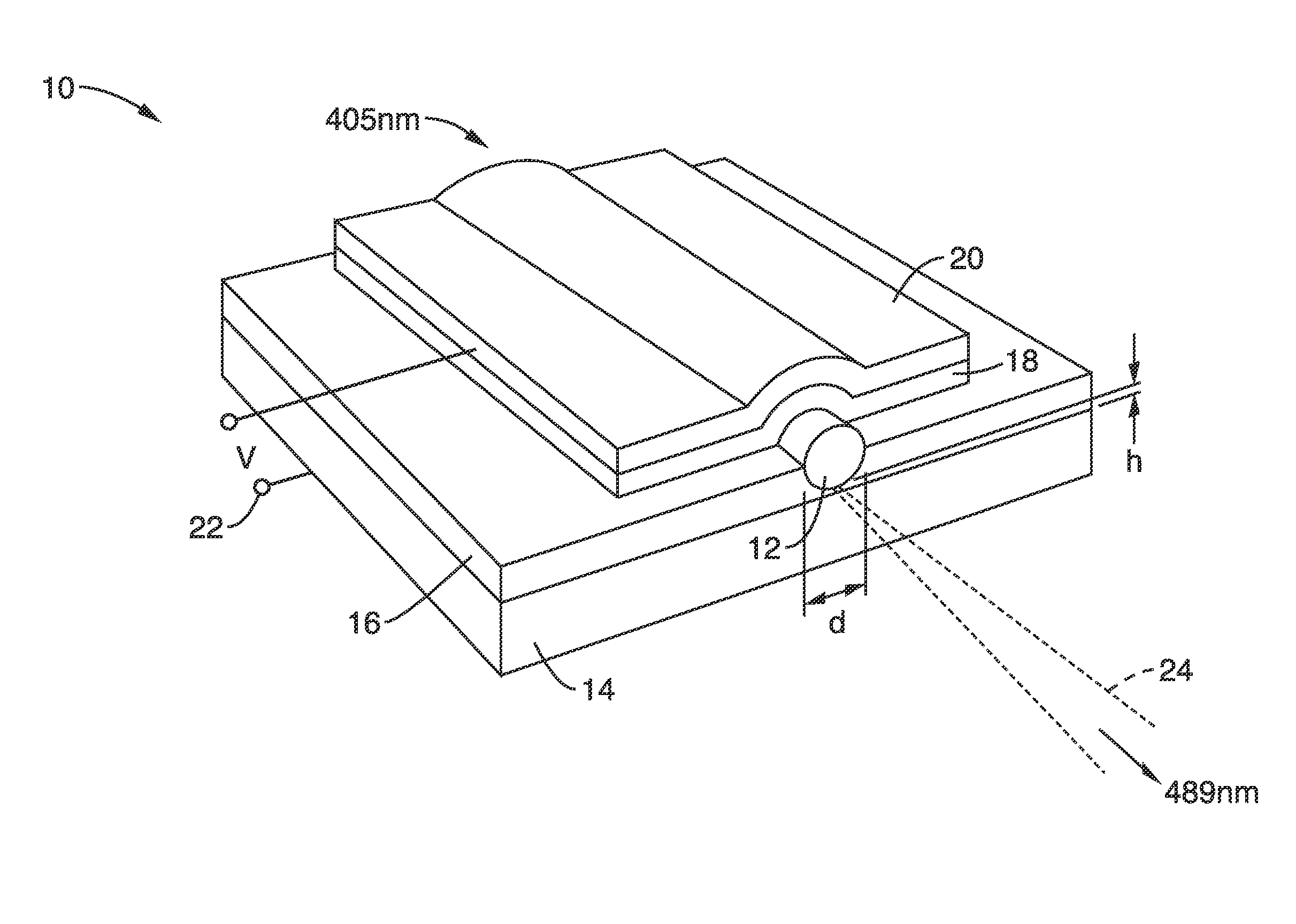
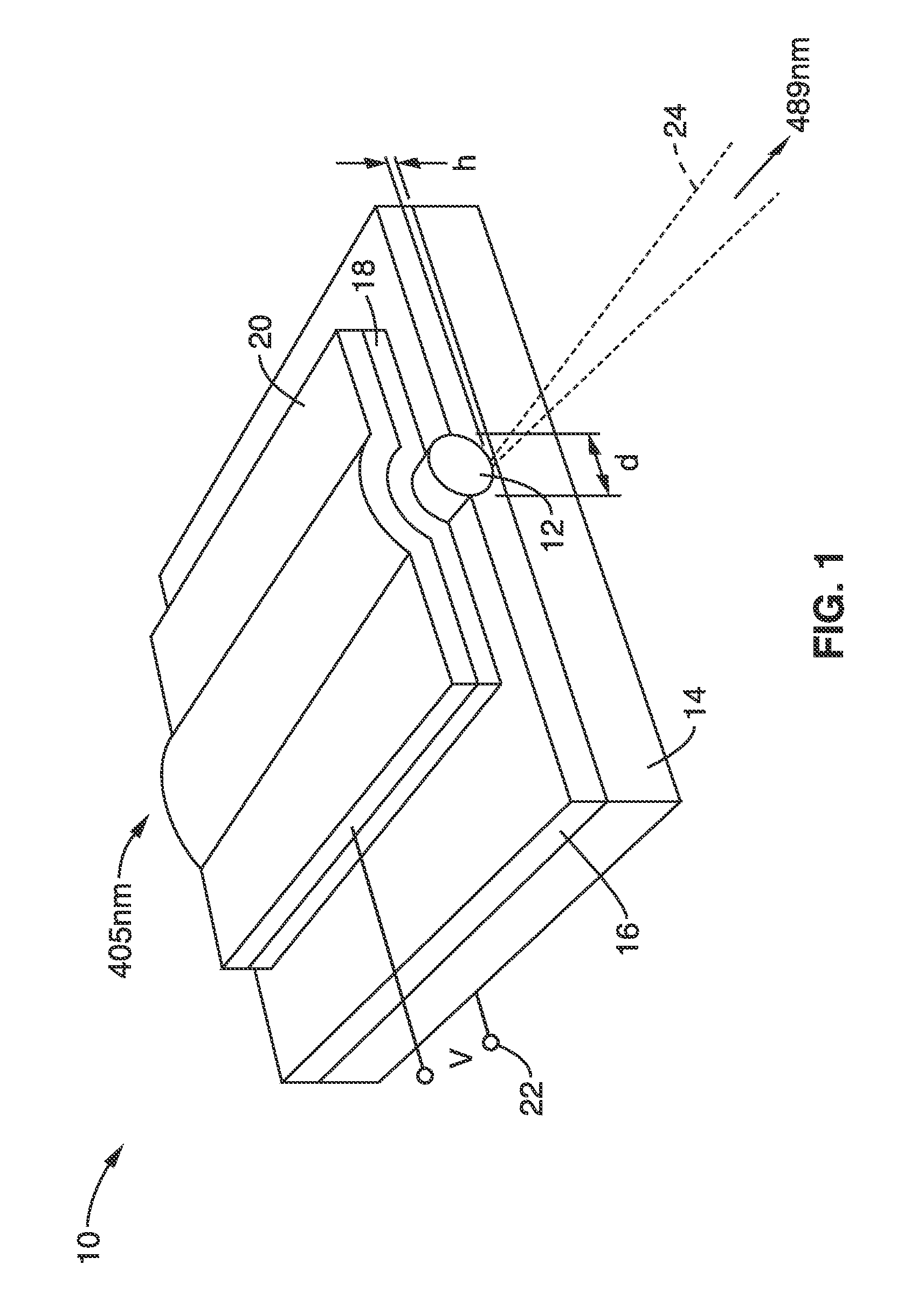
[0123]2. The laser source of embodiment 1, wherein at least a portion of the electron carrier population travel from the metal substrate through the low-refraction index gap to the semiconductor material.

[0124]3. The laser source of embodiment 1, wherein the laser source supports a plasmonic mode having a mode size smaller than λ / 2 in at least one dimension of the mode.

embodiment 3

[0125]4. The laser source of embodiment 3, wherein the laser source supports a plasmonic mode having a mode size smaller than λ / 20 in at least one dimension of the mode.

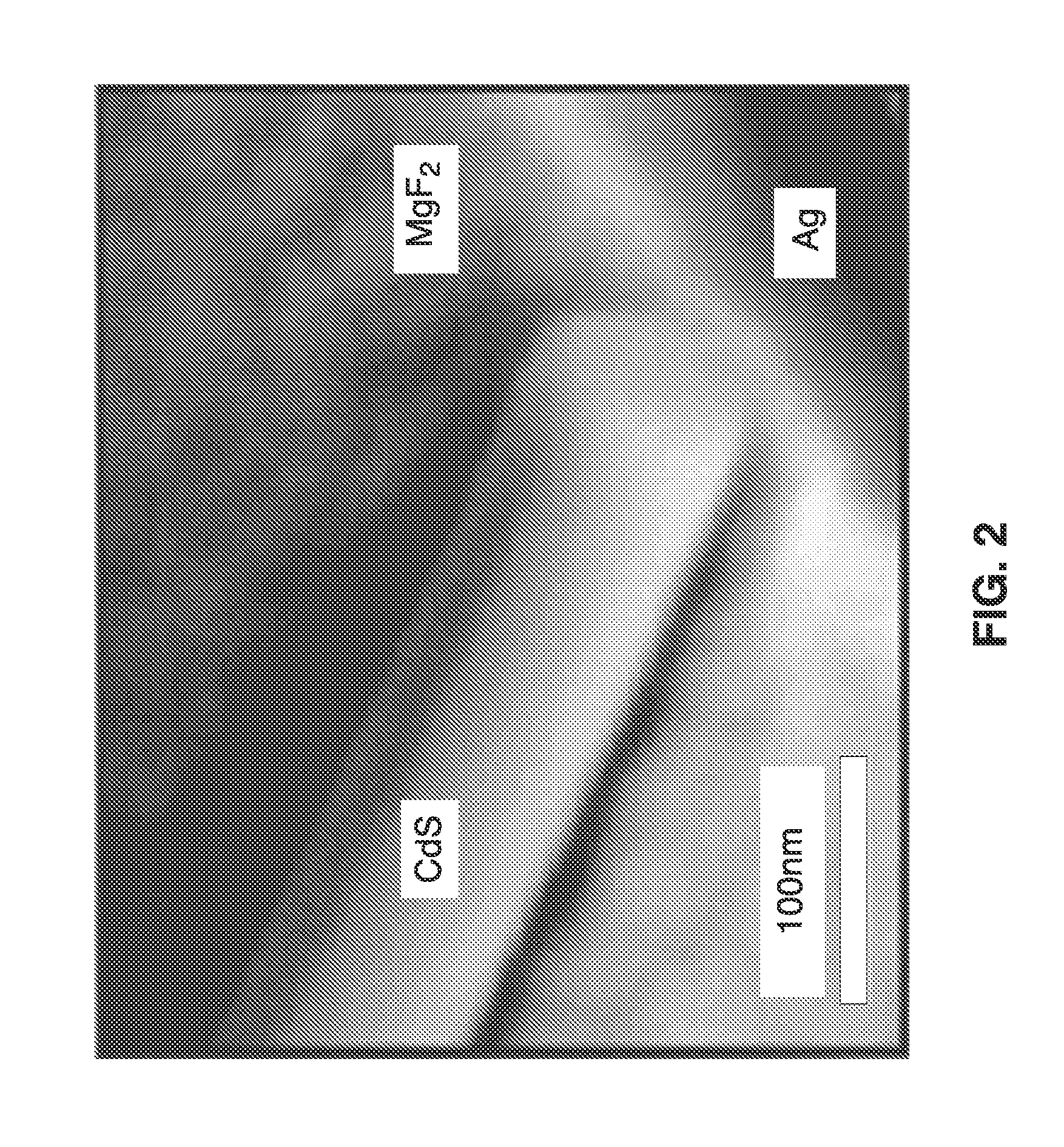
[0126]5. The laser source of embodiment 1, wherein the low-refraction index gap comprises a layer of material having a thickness that ranges between approximately 1 nm and approximately 100 nm.

embodiment 5

[0127]6. The laser source of embodiment 5, wherein the low-refraction index gap comprises a layer of material having a thickness that ranges between approximately 2 nm and approximately 50 nm.


PUM


Abstract

Hybrid plasmonic waveguides are described that employ a high-gain semiconductor nanostructure functioning as a gain medium that is separated from a metal substrate surface by a nanoscale thickness thick low-index gap. The waveguides are capable of efficient generation of sub-wavelength high intensity light and have the potential for large modulation bandwidth >1 THz.

Description

CROSS-REFERENCE TO RELATED APPLICATIONS[0001]This application is a 35 U.S.C. §111(a) continuation of PCT international application number PCT / US2011 / 045633 filed on Jul. 27, 2011, incorporated herein by reference in its entirety, which is a nonprovisional of U.S. provisional patent application Ser. No. 61 / 367,924 filed on Jul. 27, 2010, incorporated herein by reference in its entirety. Priority is claimed to each of the foregoing applications.[0002]The above-referenced PCT international application was published as PCT International Publication No. WO 2012 / 015990 on Feb. 2, 2012 and republished on Jun. 21, 2012, and is incorporated herein by reference in its entirety.STATEMENT REGARDING FEDERALLY SPONSORED RESEARCH OR DEVELOPMENT[0003]This invention was made with Government support under Grant No. 67N-1069929 awarded by the Air Force Office of Scientific Research (AFOSR) MURI and Grant No. CMMI-0751621 awarded by the National Science Foundation Nanoscale Science and Engineering Cent...

Claims


Application Information

Patent Timeline
IPC IPC(8): H01S5/30
CPCH01S5/0206H01S5/041H01S5/1046H01S5/2031B82Y20/00H01S5/341H01S5/4031H01S5/30H01S5/22
Inventor ZHANG, XIANGSORGER, VOLKER JENDRIKOULTON, RUPERT FRANCIS MAXIMILLIANMA, REN-MIN
Owner RGT UNIV OF CALIFORNIA
Why Eureka
Try Eureka