
Graphene Films and Methods of Making Thereof

a graphene film and graphene technology, applied in the field of graphene films and methods of making graphene films, can solve the problems of low yield of typically sub-100 m graphene flakes, unsuitable for precise positioning of graphene structures within device architectures, and inability to scale to practical quantities

Active Publication Date: 2013-06-20
THE RES FOUND OF STATE UNIV OF NEW YORK
View PDF3 Cites 105 Cited by
  • Summary
  • Abstract
  • Description
  • Claims
  • Application Information

AI Technical Summary

Benefits of technology

The patent describes a way to make graphene by using electrophoretic deposition, which is a simple and fast method to create large-area films on conductive surfaces. The method can be used to make graphene and functionalized graphene, which means that the graphene has been chemically modified. Overall, this patent provides a way to make high-quality graphene films on conductive materials.

Problems solved by technology

Several approaches have been reported for obtaining single graphene sheets on substrates including the original micromechanical cleavage “scotch tape” method involving the repeated exfoliation of graphite mesas; however, this method gives a very low yield of typically sub-100 μm graphene flakes masked by hundreds of thicker flakes of graphite and is thus unsuitable for precise positioning of graphene structures within device architectures and for scaling to practical quantities.

Method used


Image

  • Graphene Films and Methods of Making Thereof
  • Graphene Films and Methods of Making Thereof
  • Graphene Films and Methods of Making Thereof

Examples


example 1

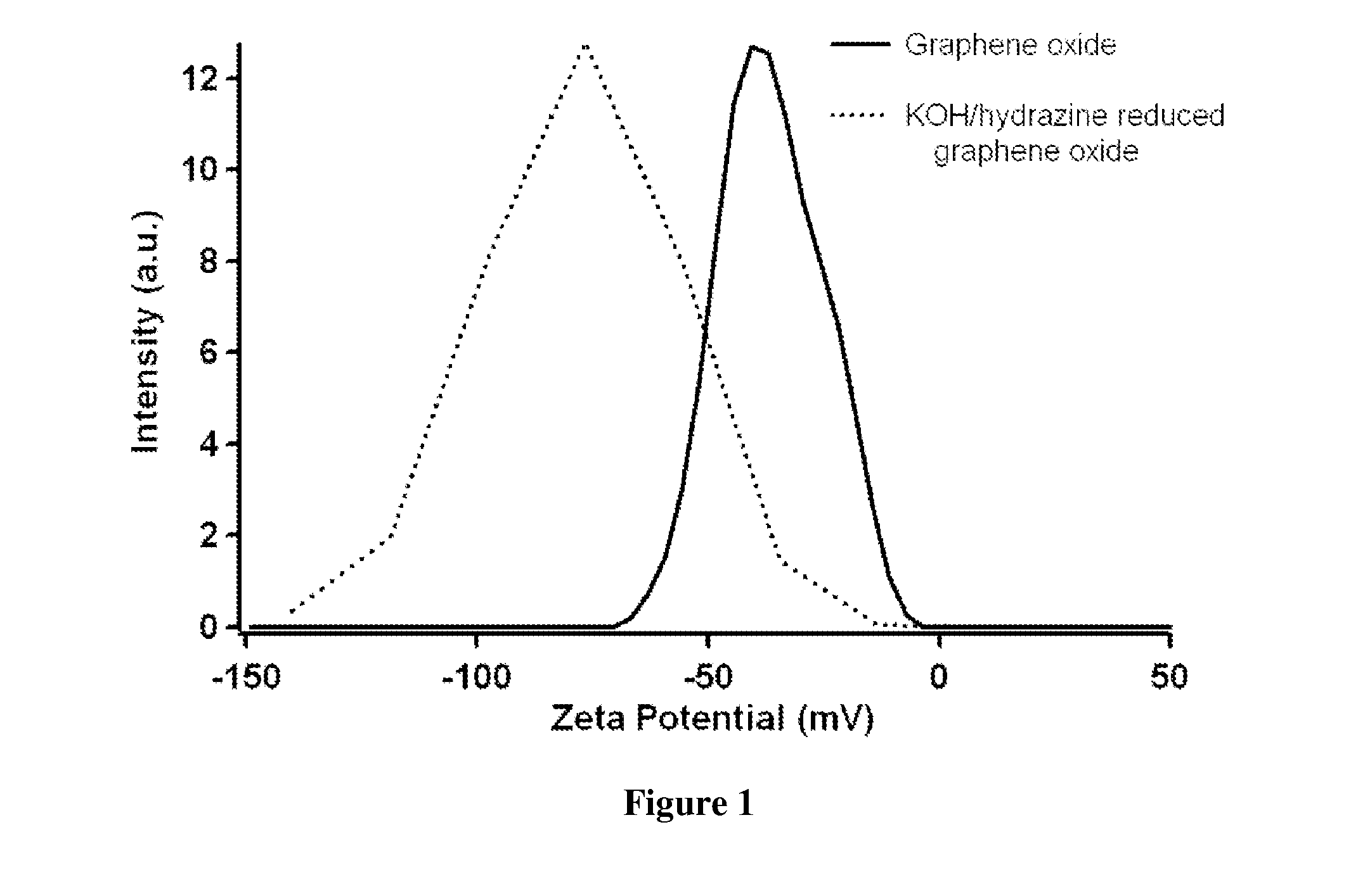
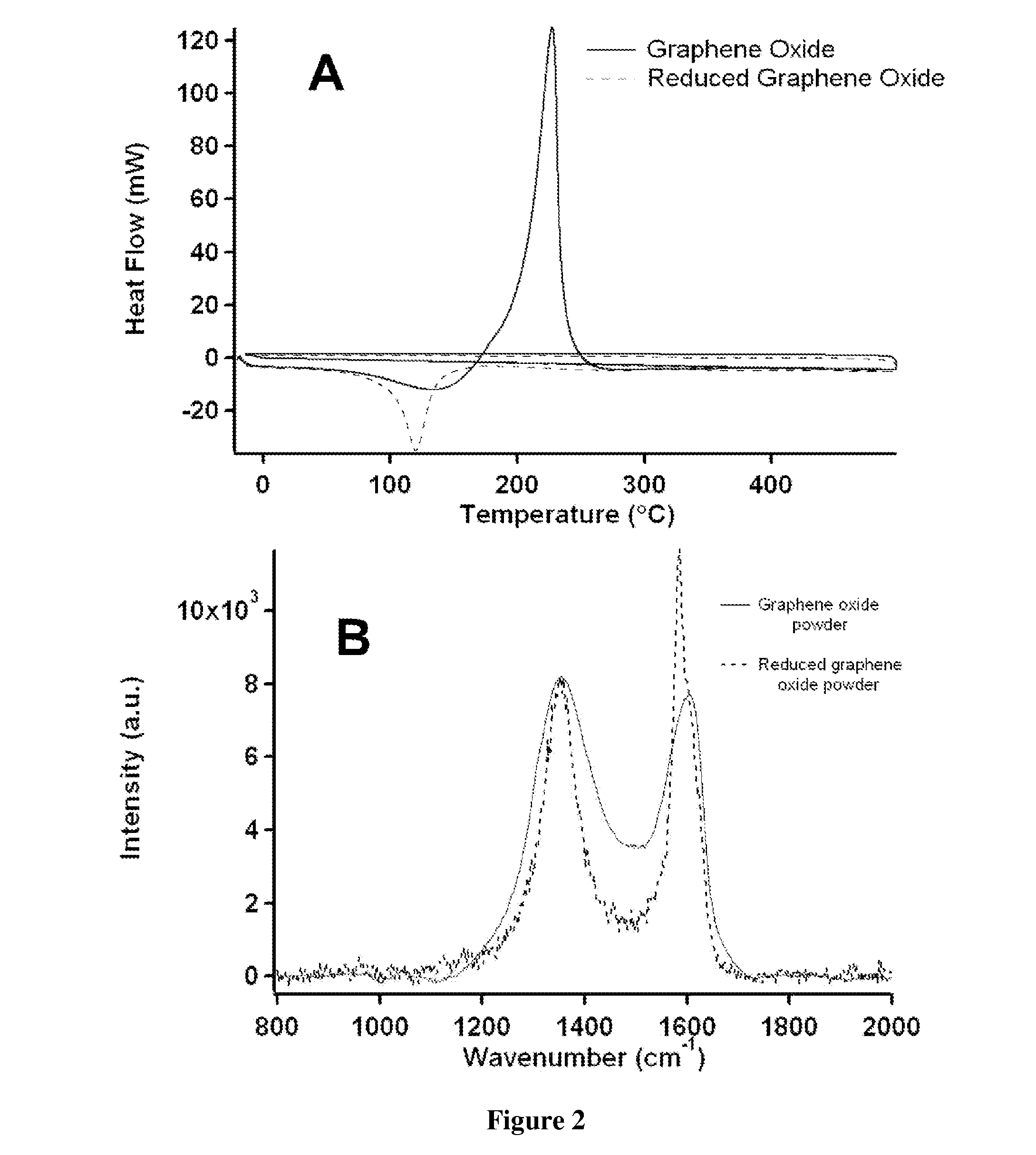
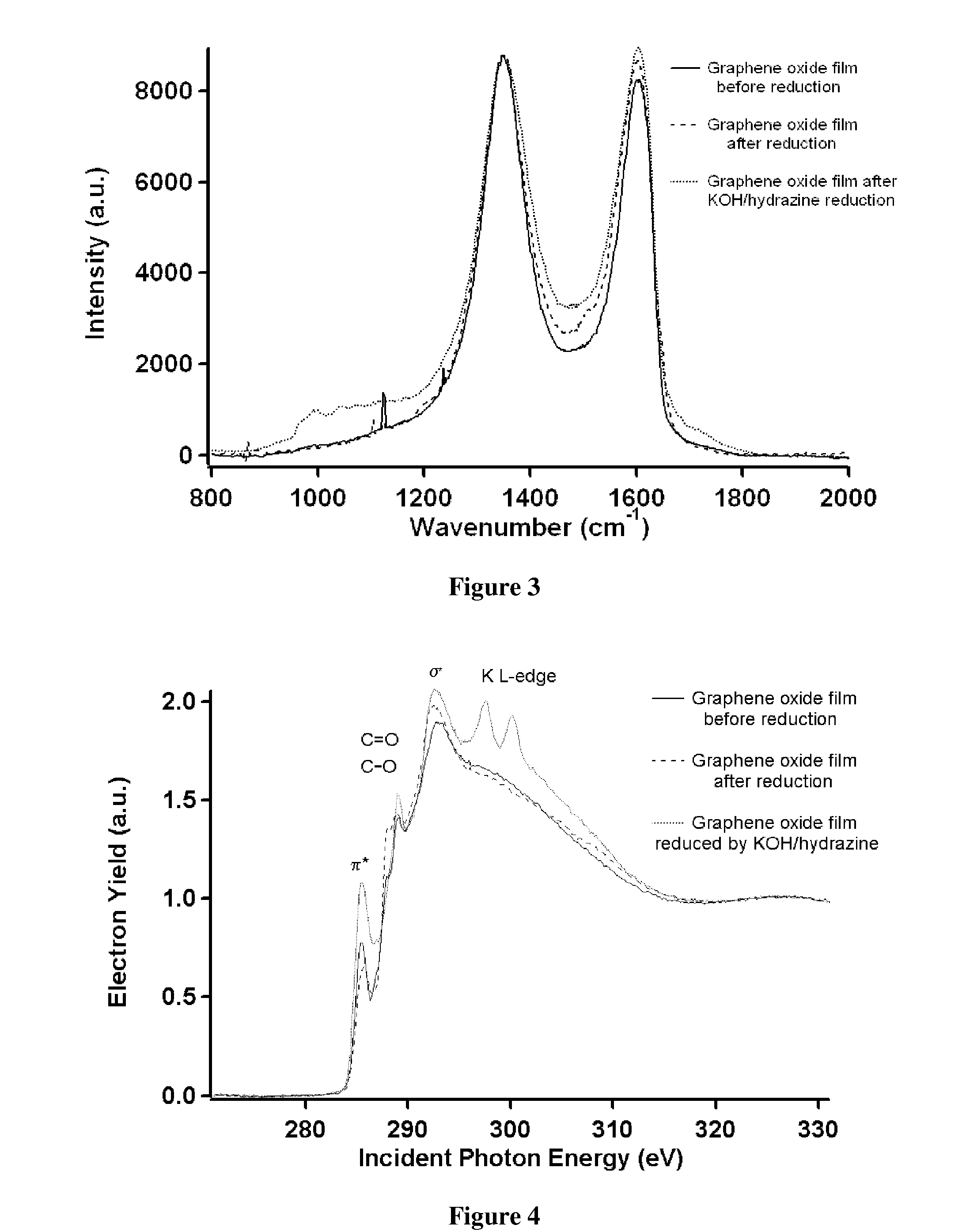
[0064]Provided in this example are two approaches for fabricating large-area graphene samples on conductive and non-conductive substrates. In the first approach, electric fields are used to deposit oriented conformal graphene films on conducting substrates such as stainless steel, carbon steel, and indium tin oxide (ITO). In the second approach filtration and transfer printing are combined to obtain large-area graphene films on glass and polyimide substrates. The approach pertains to a facile and fully scalable electrophoretic deposition approach for the fabrication of smooth conformal films of graphene oxide and chemically derived graphene sheets on conductive substrates. Two distinct approaches for fabricating chemically derived graphene films by electrophoretic deposition are disclosed. In the first approach, exfoliated graphene oxide sheets are electrophoretically deposited onto an ITO-coated glass substrate from aqueous solution and the resulting films are reduced by dipping in...

example 2

[0103]Several examples of the reduction of graphene oxide by post-processing treatment with reducing agents. Data for these films is shown in Table 3. The provided values represent the sheet resistance measured for ˜100 nm thick graphene oxide films reduced by different reducing agents. A lower sheet resistance value indicates better recovery of the conjugated graphene structure. A higher dichroic ratio value indicates better alignment of the graphene films on the substrate.

TABLE 3Sheet ResistanceReducing AgentDichroic Ratio(kohm / square)Vapor hydrazine, annealed−0.69 ± 0.08 6500 ± 1000Vapor hydrazine, not annealed−0.33 ± 0.0514000 ± 1500Liquid phenylhydrazine−0.33 ± 0.042000 ± 500Sodium borohydride−0.67 ± 0.03 5000 ± 3000Aqueous hydrazine−0.61 ± 0.0728000 ± 2400Vapor phenylhydrazine, annealed−0.04 ± 0.10 250 ± 100Vapor hydrazine, not annealed−0.47 ± 0.05134000 ± 30000No reducing agent−0.42 ± 0.03NA


PUM


Abstract

Provided are methods for forming graphene or functionalized graphene thin films. Also provided are graphene and functionalized graphene thin films formed by the methods. For example, electrophoretic deposition methods and stamping methods are used. Defect-free thin films can be formed. Patterned films can be formed. The methods can provide conformal coatings on non-planar substrates.

Description

CROSS-REFERENCE TO RELATED APPLICATIONS[0001]This application claims priority to U.S. provisional patent application No. 61 / 355,290, filed Jun. 16, 2010, the disclosure of which is incorporated herein by reference.FIELD OF THE INVENTION[0002]The present invention generally relates to graphene films and methods of making graphene films. More particularly, the present invention relates to electrophoretic and physical methods of making graphene films.BACKGROUND OF THE INVENTION[0003]Recent experimental progress in developing methods for fabricating strictly 2D crystals that were previously believed to be thermodynamically unstable have lead to remarkable paradigm-shifting discoveries in solid state physics. Graphene, a single layer of graphite, has attracted tremendous interest from the scientific community owing to its remarkable properties such as the room-temperature half-integer quantum Hall effect, the massless Dirac fermion nature and extremely high mobilities of its charge carri...

Claims


Application Information

Patent Timeline
Patent Type & Authority Applications(United States)
IPC IPC(8): C01B31/04C25D13/00
CPCB82Y30/00B82Y40/00C01B31/0469C01B31/0476C01B2204/30C25D13/22C01B31/043C01B31/0438C25D13/00C25D13/02C25D13/18C01B2204/32C01B32/23C01B32/19C01B32/192H01G11/36C01B32/182C01B32/198
Inventor BANERJEE, SARBAJITLEE, VINCENTWHITAKER, LUISA
Owner THE RES FOUND OF STATE UNIV OF NEW YORK
Learn More