

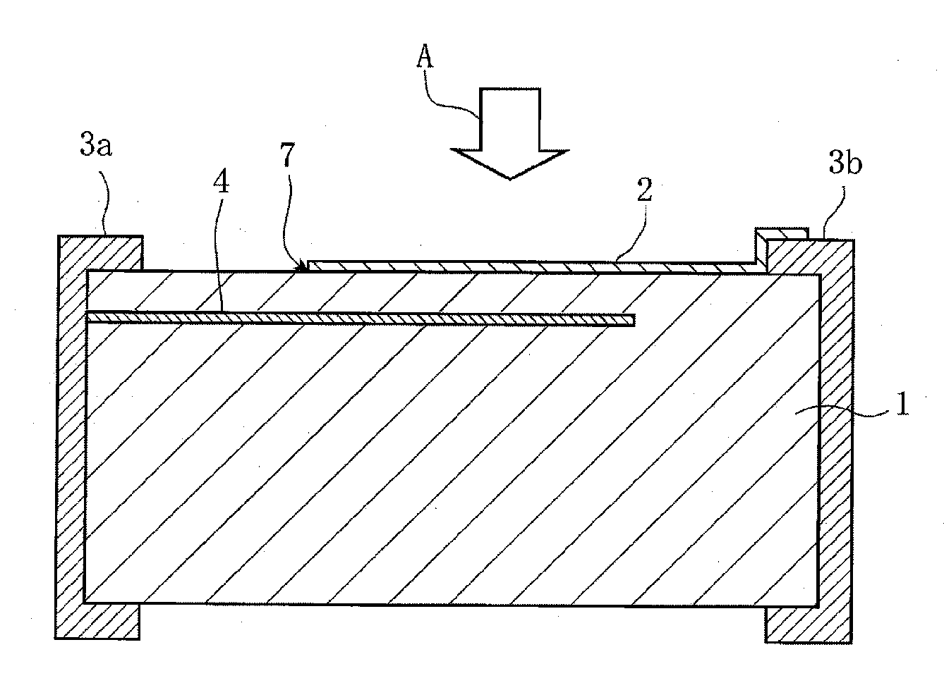
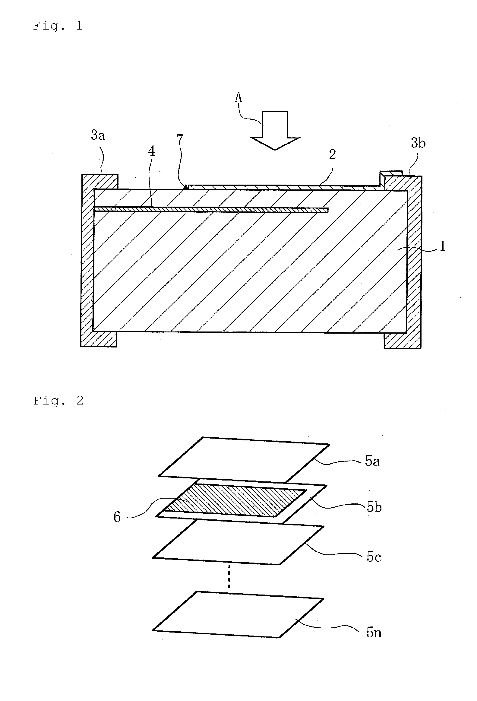
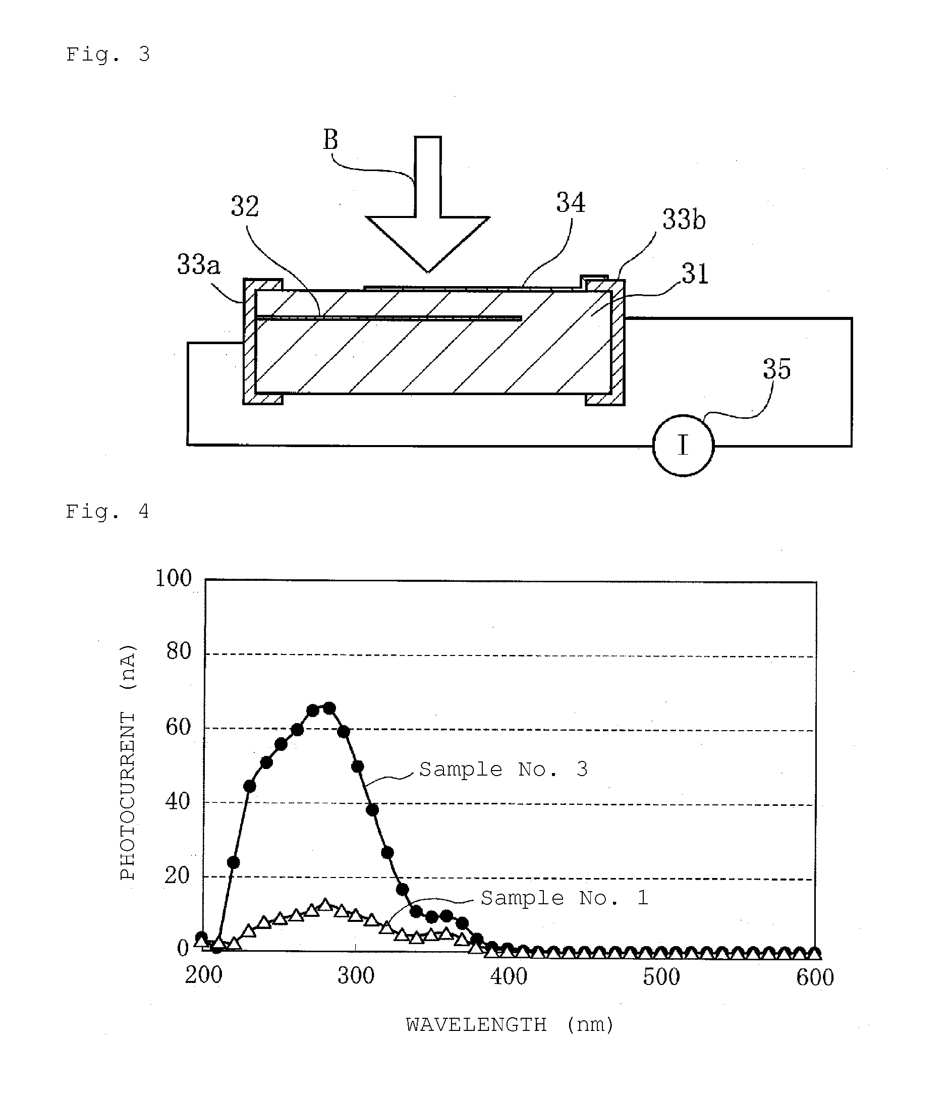
Ultraviolet Sensor and Method for Manufacturing the Same
a technology of ultraviolet light and sensor, applied in the field of ultraviolet light sensor, can solve the problems low light transmittance, and reduced light transmittance, and achieve the effect of low light absorption efficiency and decreased light transmittan
- Summary
- Abstract
- Description
- Claims
- Application Information
AI Technical Summary
Benefits of technology
Problems solved by technology
Method used
Image

Examples
examples
[0109][Preparation of Sample]
[0110](Sample Nos. 2 to 6)
[0111][Preparation of ZnO Sintered Body]
[0112]ZnO serving as a principal component and Ga2O3 as a doping agent were weighed so that compounding ratios of these compounds were 99.9 mol % and 0.1 mol %, respectively. Then, after pure water was added to these weighed compounds, the resulting mixture was mixed and pulverized in a ball mill using PSZ beads as a pulverizing medium to obtain a slurry-like mixture of particles having an average particle diameter of 0.5 μm or less. Subsequently, after the slurry-like mixture was dehydrated and dried, the slurry was granulated to have a particle diameter of about 50 μm, and then resulting grains were calcinated for 2 hours at 1200° C. to obtain a calcined powder.
[0113]Next, after pure water was again added to the calcined powder thus obtained, the resulting mixture was mixed and pulverized in a ball mill using PSZ beads as a pulverizing medium to obtain a slurry-like pulverized material o...
PUM
| Property | Measurement | Unit |
|---|---|---|
| surface roughness | aaaaa | aaaaa |
| surface roughness | aaaaa | aaaaa |
| wavelength band | aaaaa | aaaaa |
Abstract
Description
Claims
Application Information