Method of making a non-volatile double gate memory cell

Inactive Publication Date: 2013-07-18
COMMISSARIAT A LENERGIE ATOMIQUE ET AUX ENERGIES ALTERNATIVES
View PDF3 Cites 10 Cited by
  • Summary
  • Abstract
  • Description
  • Claims
  • Application Information

AI Technical Summary

Benefits of technology

[0026]In this way the bottom of the difference of levels of the other layer is at a level equal to or higher than the tops of the difference of levels of a semiconductor material. The said other layer therefore makes it possible, during the step of chemical mechanical polishing, to strip a substantial part of the polycrystalline silicon layer situated above the pattern without for all that, stripping this layer on the sidewalls of the relief of the gate of the control transistor. The width of the pattern forming a spacer is therefo

Problems solved by technology

However, such memories exhibit disadvantages that limit the reduction of their dimensions.
The prolonged use of such a memory, in other words the repetition of write and erasure cycles, eventually generates defects in the tunnel oxide, which tend to evacuate the charges trapped in the floating gate.
Similarly, a large SILC or leakage current affects the retention time of the charges in the floating gate.
In practice, it is therefore difficult to reduce the thickness of the tunnel oxide of these memories to smaller than 8 nanometers or nm (1 nm=10−9 meter) without allowing the SILC to become a critical phenomenon for storage.
In addition, by reducing the dimensions of such a memory cell, the parasitic coupling between the floating gates of two adjacent cells of the same memory becomes large and may therefore degrade the reliability of the memory.
One of the difficulties for producing these memories then concerns the control of the relative position of the gates, the gate of the control transistor and the control gate of the memory transistor relative to one another.
Poor control of the relative positions of the two gates therefore translates into poor control of the e

Method used


Image

  • Method of making a non-volatile double gate memory cell
  • Method of making a non-volatile double gate memory cell
  • Method of making a non-volatile double gate memory cell

Examples


Example

[0035]The attached drawings are given by way of examples and are not limitative of the invention.

DETAILED DESCRIPTION OF THE INVENTION

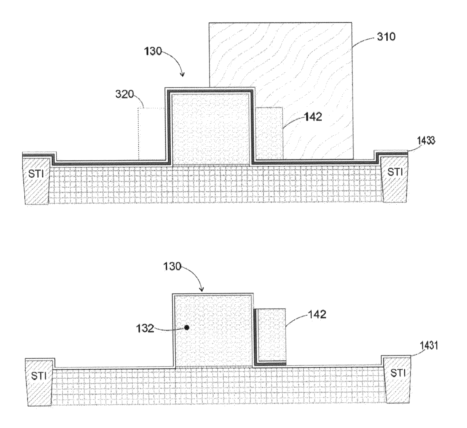
[0036]It is recalled that one of the objectives of the invention is to obtain a broader zone for defining a contact area, thus making it possible to position a via for connection with the upper circuitry layers more easily on the control gate of the memory transistor.

[0037]It is clarified that, within the scope of the present patent application, the term “on” does not necessarily mean “in contact with”. Thus, for example, the deposition of a layer of polysilicon on a layer of insulator does not necessarily mean that the layer of polysilicon is directly in contact with the layer of insulator but that means that it covers it at least partly, either by being directly in contact therewith or by being separated therefrom by another layer or another element.

[0038]Before beginning a detailed review of embodiments of the invention, optional characteristics th...


PUM


Abstract

A method of making a non-volatile double-gate memory cell. A gate of the control transistor is formed with a relief on a substrate. A control gate of the memory transistor is formed with a layer of a semiconductor material covering relief. The method includes chemical mechanical polishing (CMP) so as to strip, above the relief another layer and part of the layer of a semiconductor material; stripping of the remaining other layer on both sides of the relief, etching of the layer of a semiconductor material so as to strip this material above the relief and to leave only a pattern on at least one sidewall of the relief.

Description

TECHNICAL FIELD OF THE INVENTION[0001]The invention relates to the field of electronic memory devices or memories of non-volatile type. It has particularly advantageous application in the field of electronic memories of double-gate flash type comprising a control gate, also referred to as gate of the control transistor, and a memory gate, also referred to as control gate of the memory transistor.PRIOR ART[0002]There exist several types of non-volatile memories, in other words memories that preserve stored information in the absence of electrical supply and can be written and / or erased electrically:[0003]EPROMS, for the English “Erasable Programmable Read Only Memories”, in other words “erasable and programmable (read only) permanent memories”, the contents of which may be written electrically but which must be subjected to ultraviolet (UV) radiation to erase the information stored therein.[0004]EEPROMS, for the English “Electrically Erasable Programmable ROMs”, in other words “elect...

Claims


Application Information

Patent Timeline
IPC IPC(8): H01L29/66H01L29/788
CPCH01L21/28273H01L21/28282H01L29/4234H01L29/788H01L29/792H01L29/66825H01L29/66833H01L29/40117H01L29/40114
Inventor CHARPIN-NICOLLE, CHRISTELLE
Owner COMMISSARIAT A LENERGIE ATOMIQUE ET AUX ENERGIES ALTERNATIVES
Why Eureka
Try Eureka