

Magnetron sputtering apparatus and film forming method
a sputtering device and sputtering technology, applied in the direction of electrolysis components, vacuum evaporation coatings, coatings, etc., can solve the problems of difficult to obtain difficult to achieve the uniform thickness of film, and difficult to achieve the uniform thickness of thin film by using a reactive sputtering device. achieve the effect of high in-plane uniformity
- Summary
- Abstract
- Description
- Claims
- Application Information
AI Technical Summary
Benefits of technology
Problems solved by technology
Method used
Image

Examples
first embodiment
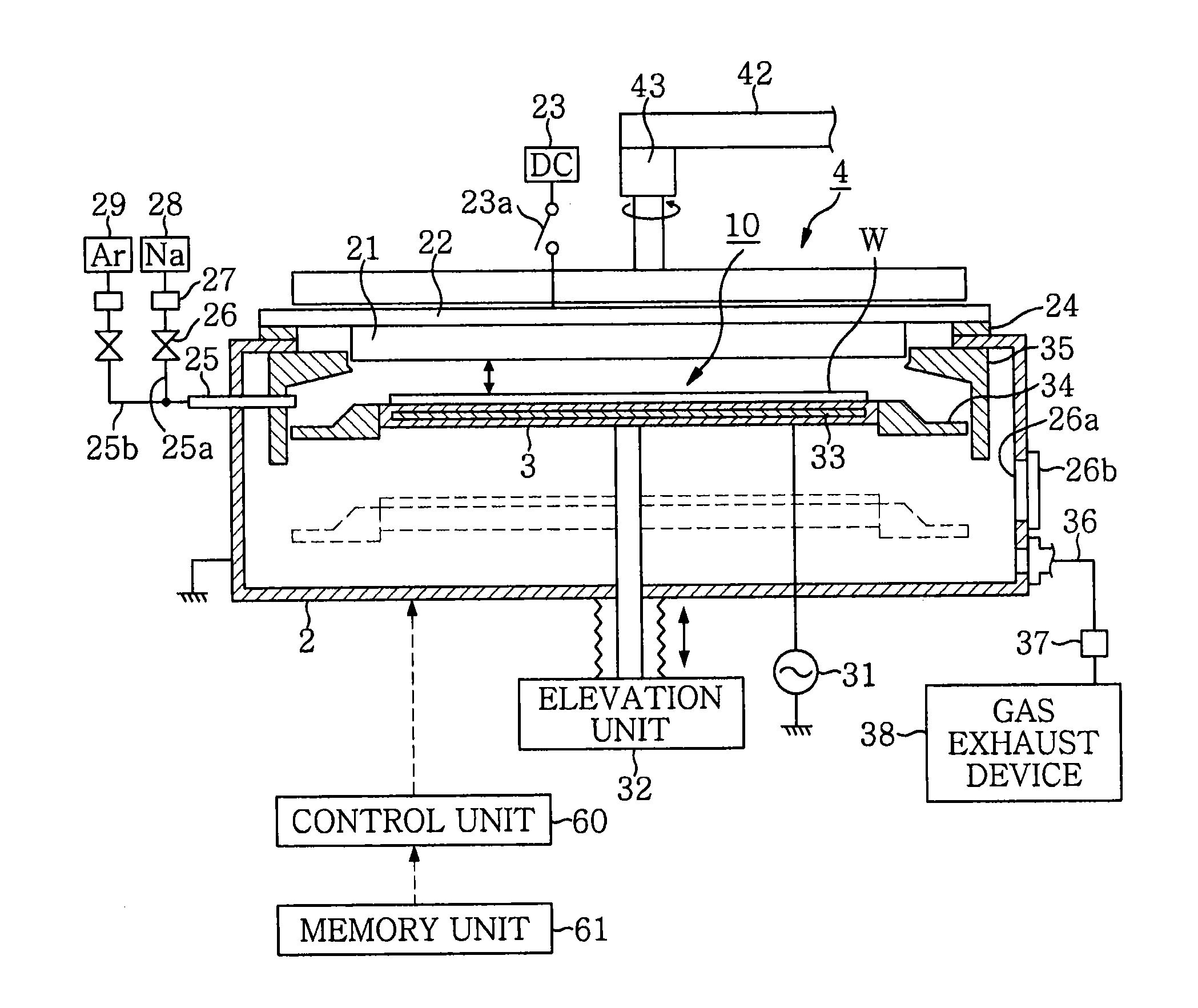
[0043]A magnetron sputtering apparatus in accordance with a first embodiment of the present invention will be described with reference to FIGS. 1 to 16 which form a part hereof.
[0044]First to provide an overview explanation of the magnetron sputtering apparatus, as shown in FIG. 1, this apparatus includes a vacuum chamber 2 for accommodating a wafer w therein; and a target 21, made of e.g. titanium (Ti) or the like, which is provided on the upper side of the vacuum chamber 2. The magnetron sputtering apparatus serves to facilitate the sputtering of the target 21 by a magnetron discharge, which is generated by a magnetic field (cusp magnetic field 100) and an electric field. Also, as shown in FIGS. 12A and 12B of which will be described later in greater detail, by sequentially switching between positions P1 to P4 where a magnetic field is generated at the central and outer periphery sides of the wafer w, it is possible to obtain an in-plane uniform film thickness and film quality of ...
second embodiment
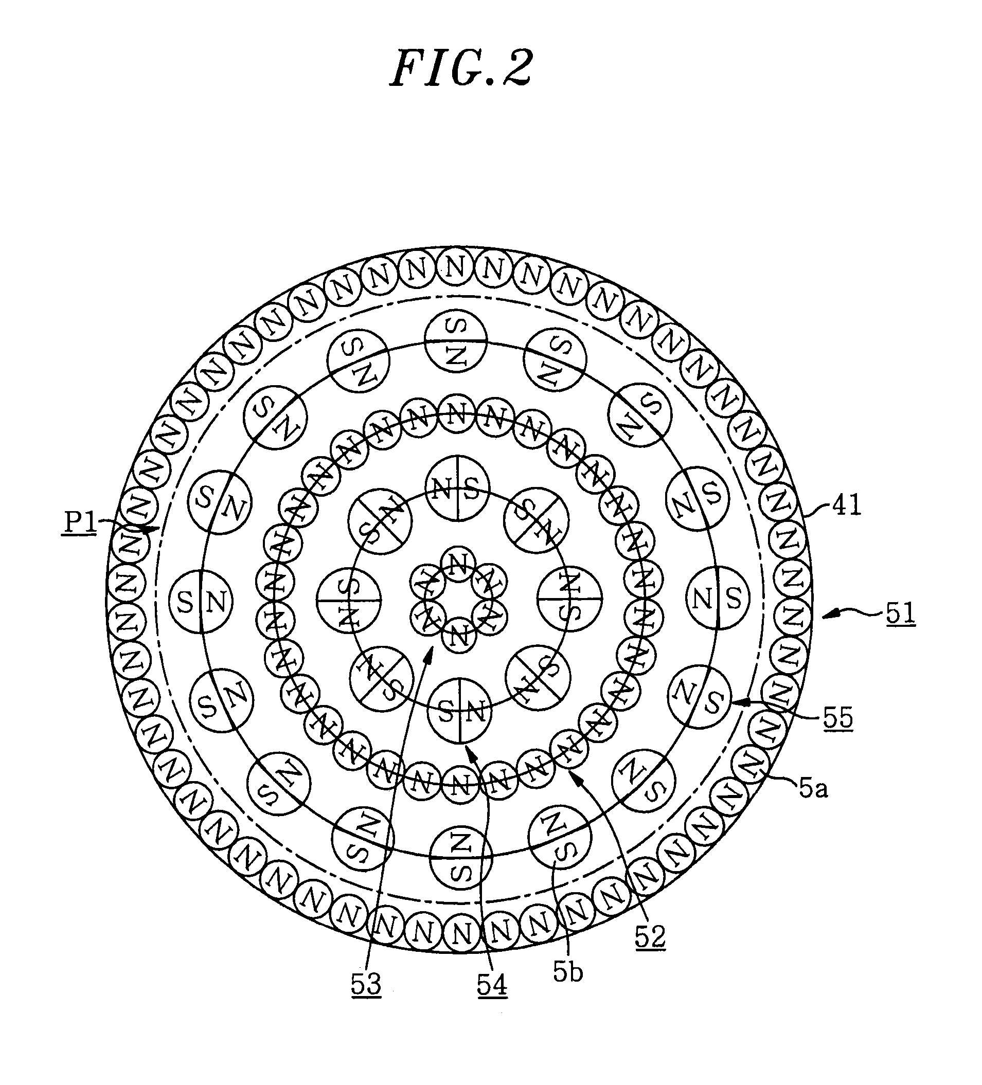
[0094]According to the first embodiment described above, in the case where the magnet array body 4 is not eccentrically rotated, that is, the magnet array body 4 is rotated around the vertical axis extending through the center of the wafer W, the erosion of the target 21 is difficult to generate at the bottom positions of the main ring-shaped magnet arrays 51 to 53.
[0095]Further, even though the magnetic fields generated by the auxiliary magnet arrays are in rotational positions which inhibit sputtering, an unintended, not-so-small erosion may occur because some of the magnetic fields are formed at opposite sides of a radius direction. Therefore, in the second embodiment described below, the target 21 is configured in such a way that the erosion occurs uniformly over the surface of the target 21 even when the magnet array body 4 is not eccentrically rotated. Furthermore, the intended ring-shaped erosion can be accurately formed.
[0096]Specifically, as shown in FIG. 17, each of the ri...
PUM
| Property | Measurement | Unit |
|---|---|---|
| distance | aaaaa | aaaaa |
| distance | aaaaa | aaaaa |
| magnetic flux density | aaaaa | aaaaa |
Abstract
Description
Claims
Application Information