Lighting-emitting device with nanostructured layer and method for fabricating the same

a light-emitting device and nano-structure technology, applied in the direction of polycrystalline material growth, crystal growth process, chemically reactive gas, etc., can solve the problems of high vsub>f, high vsub>f, and high vsub>f, so as to improve the internal quantum efficiency of the light-emitting device, reverse voltage and forward voltage, and reduce the epitaxy time. , the effect of improving the internal quantum efficiency

Inactive Publication Date: 2013-07-25
ZHEJIANG INVENLUX TECH
View PDF6 Cites 30 Cited by
  • Summary
  • Abstract
  • Description
  • Claims
  • Application Information

AI Technical Summary

Benefits of technology

[0005]Disclosed herewith are a light emitting device having a nanostructured layer with nanovoids and method of manufacturing the same to improve light-emitting device's internal quantum efficiency, light extraction efficiency, reverse voltage, and forward voltage in a consist

Problems solved by technology

Compromises are to be made as improving one aspect is usually at the expense of the other aspect.
For example, using heavily doped n-GaN (Si doping level up to 2×1019 cm−3 has been employed in U.S. Pat. Nos. 6,630,692 and 7,026,653) for better current spreading can reduce device Vf, howe

Method used


Image

  • Lighting-emitting device with nanostructured layer and method for fabricating the same
  • Lighting-emitting device with nanostructured layer and method for fabricating the same
  • Lighting-emitting device with nanostructured layer and method for fabricating the same

Examples


Embodiment Construction

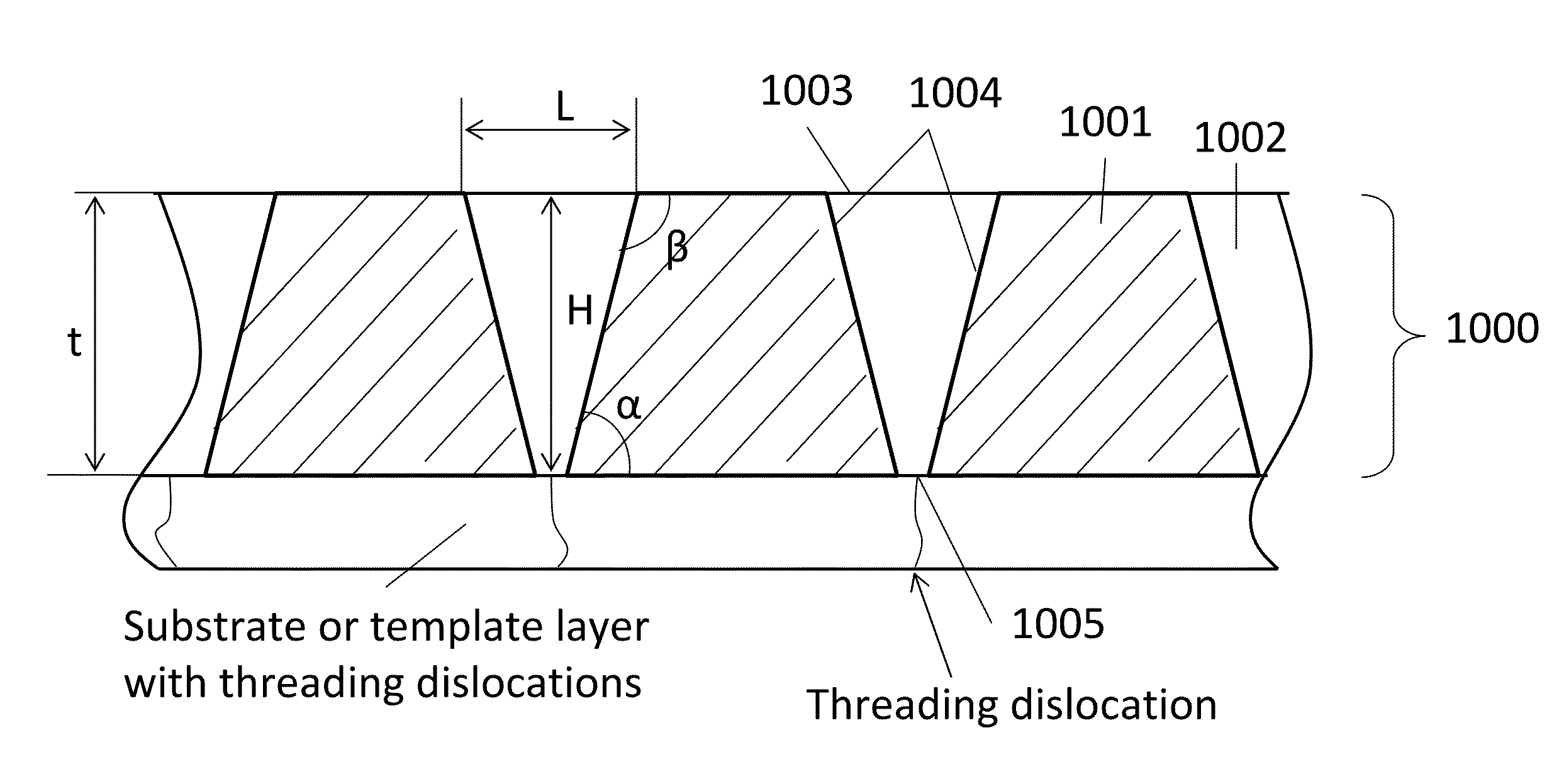
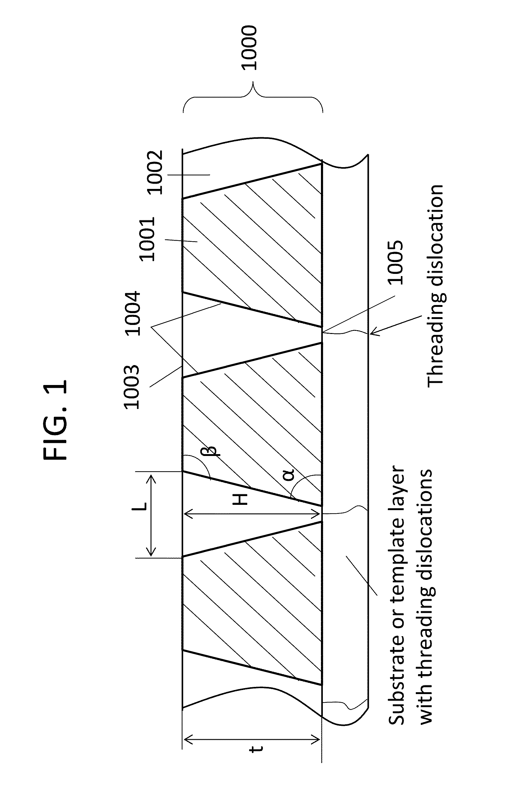
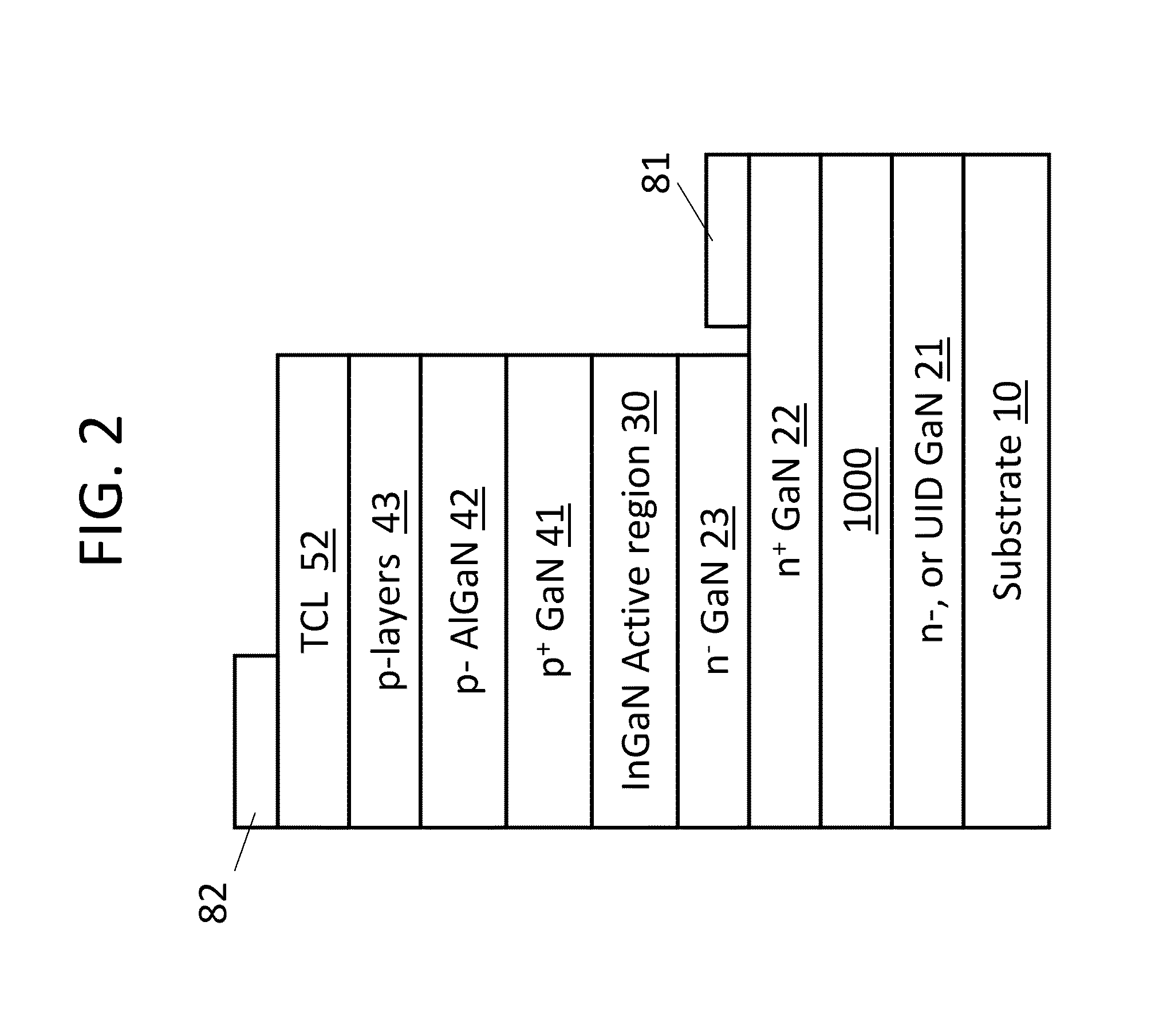
[0055]Throughout the specification, the term III-nitride or nitride in general refers to metal nitride with cations selecting from group IIIA of the periodic table of the elements. That is to say, III-nitride includes AlN, GaN, InN and their ternary (AlGaN, InGaN, InAlN) and quaternary (AlInGaN) alloys. III-nitride or nitride can also include small compositions of transition metal nitride such as TiN, ZrN, HfN with molar fraction not larger than 10%. For example, III-nitride or nitride may include AlxInyGazTi(1-x-y-z)N, AlxInyGazZr(1-x-y-z)N, AlxInyGazHf(1-x-y-z)N, with (1-x-y-z)≦10%. A III-nitride layer or active-region means that the layer or active-region is made of III-nitride semiconductors.

[0056]Throughout the specification, the term II-VI semiconductor in general refers to semiconductors with cations and anions respectively selected from group IIB and group VIA of the periodic table of the elements. That is to say, II-VI semiconductors include ZnO, ZnS, ZnSe, ZnTe, CdO, CdS, ...


PUM


Abstract

A light emitting device has a nanostructured layer with nanovoids. The nanostructured layer can be provided below and adjacent to active region or on a substrate or a template below an n-type layer for the active region, so as to reduce strain between epitaxial layers in the light emitting device. A method of manufacturing the same is provided.

Description

1. FIELD OF THE INVENTION [0001]The present invention relates in general to light-emitting device having nanostructured layer, more particularly to III-nitride light-emitting device having nanostructured nitride layer, or II-VI light-emitting device having nanostructured II-VI layer, and method for fabricating the same.2. DESCRIPTION OF THE RELATED ART [0002]III-nitride based light-emitting devices such as light-emitting diodes (LEDs) are widely acknowledged as the next generation light sources and are currently emerging as strong replacement of incandescent and fluorescent lamps in general lighting. For example, the field of interest uses Cerium-doped yttrium aluminum garnet (YAG:Ce) phosphor to convert InGaN multiple-quantum-well (MQW) LED' s blue emission into white light, yielding commercial white light LEDs with luminous efficacies in the range of 80-130 lm / W. The R&D White LED luminous efficacy record reported so far has reached 183 lm / W (Y. Narukawa et al, J. Phys. D: Appl. P...

Claims


Application Information

Patent Timeline
IPC IPC(8): H01L33/32C30B25/02B82Y99/00
CPCH01L33/32B82Y20/00B82Y40/00H01L33/16
Inventor ZHANG, JIANPINGWANG, HONGMEIYAN, CHUNHUIWANG, WENLIU, YING
Owner ZHEJIANG INVENLUX TECH
Why Eureka
Try Eureka