

Epitaxy level packaging
- Summary
- Abstract
- Description
- Claims
- Application Information
AI Technical Summary
Benefits of technology
Problems solved by technology
Method used
Image

Examples
Embodiment Construction
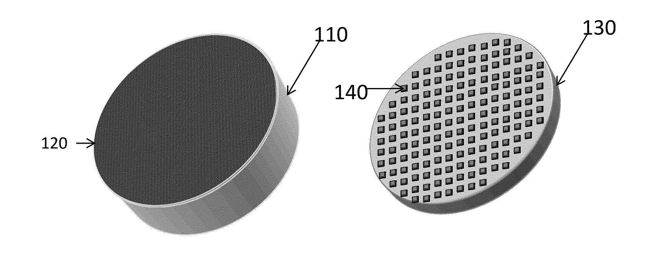
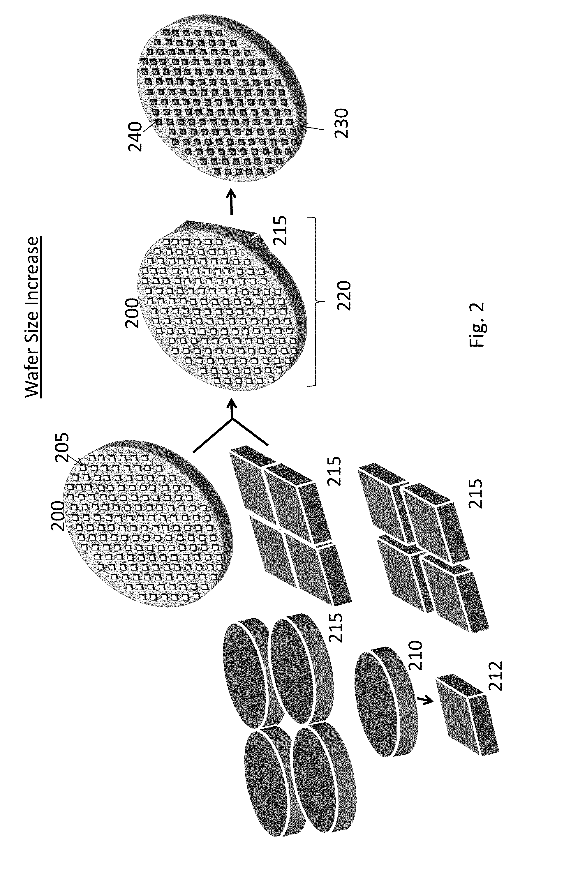
[0030]From the perspectives of material, processing, and assembly, ELP makes efficient use of compound semiconductor material by growing islands / pillars (and plateaus) of material rather than entire wafers, and further has the ability to integrate several different compound semiconductor materials (GaAs, GaN, InP, GaSb, InAs, GaP, InSb, AlN, SiC, SiGe, ZnS, ZnSe, CdTe, InGaP, InGaAs, AlGaAs, InGaN, AlGaN, etc.) on the same wafer platform (e.g. silicon) using existing wafer fabrication processes. Wafer level heterogeneous integration is readily achievable by selective masking and demasking of ELP structures (including islands) and Si regions / area either by fabricating each microsystem sequentially or fabricating multiple microsystems simultaneously by inserting / integrating modular steps of one microsystem into the flow of another microsystem at appropriate steps while preserving the electrical integrity of all microsystems. ELP can also use a uniform wafer size, and thus standardize ...
PUM
 Abstract
Description
Claims
Application Information