High frequency solid state switching for impedance matching

a solid-state switching and high-frequency technology, applied in the field of plasma processing, can solve the problems of resistive elements in the match network, bulky and expensive, pin diodes can be too slow for rf power applications, etc., and achieve the effect of reducing susceptibility and reducing curren

Active Publication Date: 2013-08-15
AES GLOBAL HLDG PTE LTD
View PDF2 Cites 53 Cited by
  • Summary
  • Abstract
  • Description
  • Claims
  • Application Information

AI Technical Summary

Benefits of technology

[0006]Exemplary embodiments of the present invention that are shown in the drawings are summarized below. These and other embodiments are more fully described in the Detailed Description section. It is to be understood, however, that there is no intention to limit the invention to the forms described in this Summary of the Invention or in the Detailed Description. One skilled in the art can recognize that there are numerous modifications, equivalents and alternative constructions that fall within the spirit and scope of the invention as expressed in the claims.
[0007]Some embodiments of the disclosure may be characterized as a circuit of a variable capacitance element of an impedance matching network. The match comprises a capacitor, a first and second diode, and a transistor. The capacitor is coupled between a first voltage line and a first node. The first diode has an anode coupled to the first node and a cathode coupled to a second node. The second diode has an anode to couple to a second voltage line and a cathode to couple to the first node. The transistor has a first, second, and control terminals. The first terminal is coupled to the second node, the second terminal is coupled to the second voltage line, and the control terminal is coupled to a controller. The capacitor is switched into the variable capacitance element when the transistor is on and switched out after the transistor is off.
[0008]Other embodiments of the disclosure may also be characterized as a circuit of a variable capacitance element of an impedance matching network. The match network includes a capacitor, a first diode, a low power DC bias, and a transistor. The capacitor is coupled between a first voltage line and a first node. The first diode has an anode coupled to the first node and a cathode coupled to a second node. The low power DC bias source provides a first DC bias to the first node via a second diode. The transistor has a first terminal, a second terminal, and a control terminal. The first terminal is coupled to the second node, the second terminal is coupled to a second voltage line, and the control terminal receives signals controlling switching of the transistor. The capacitor is switched into the variable capacitance element when the transistor is on and switched out after the transistor is off.
[0009]Other embodiments of the disclosure can be characterized as a method of switching a capacitor in and out of a variable capacitance element of an impedance matching network. The method includes turning a transistor of the variable capacitance element off. Also, charging a body capacitance of the transistor via a first diode using current from an RF signal passing through the capacitor. Further, the method includes reverse biasing the first diode with a voltage supplied by the body capacitance of the transistor after charging. Also, reducing the current from the RF signal through the capacitor to near zero amperes so as to reduce a susceptance (imaginary part of admittance calculated at the nominal operating frequency) of the variable capacitance element. Additionally, the method includes discharging the body capacitance of the transistor and forward biasing the first diode with current from the RF signal passing through the capacitor.

Problems solved by technology

The only resistive elements in a match network are typically associated with losses in non-ideal reactive and lossless components or components that do not take part in the impedance transformation such as components for sensing voltage, current, power or temperature.
However, these are bulky and expensive.
However, such PIN diodes can be too slow for RF power applications, or can require excessive power to accomplish the switching at acceptable speeds.
This in turn results in running the PIN diodes at high temperatures.
PIN diodes are also expensive and only produced by a handful of manufacturers.

Method used


Image

  • High frequency solid state switching for impedance matching
  • High frequency solid state switching for impedance matching
  • High frequency solid state switching for impedance matching

Examples


Embodiment Construction

[0022]The present disclosure relates generally to plasma processing. More specifically, but without limitation, the present disclosure relates to match networks of a power supply for generating and sustaining a plasma in, or provided to, a plasma processing chamber.

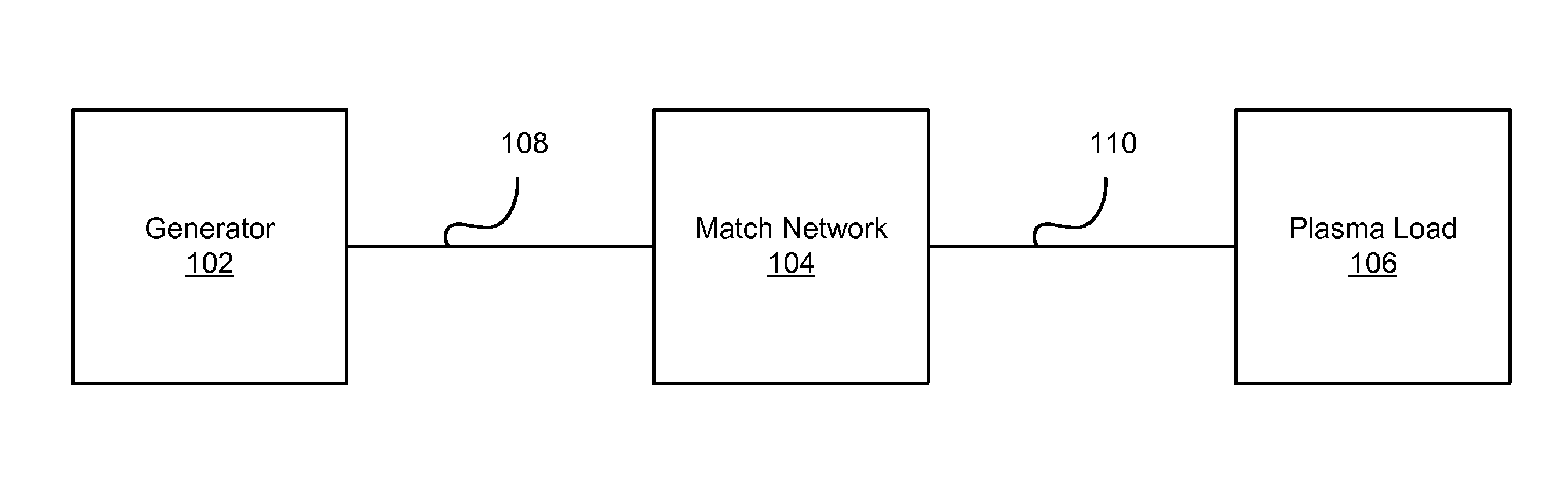
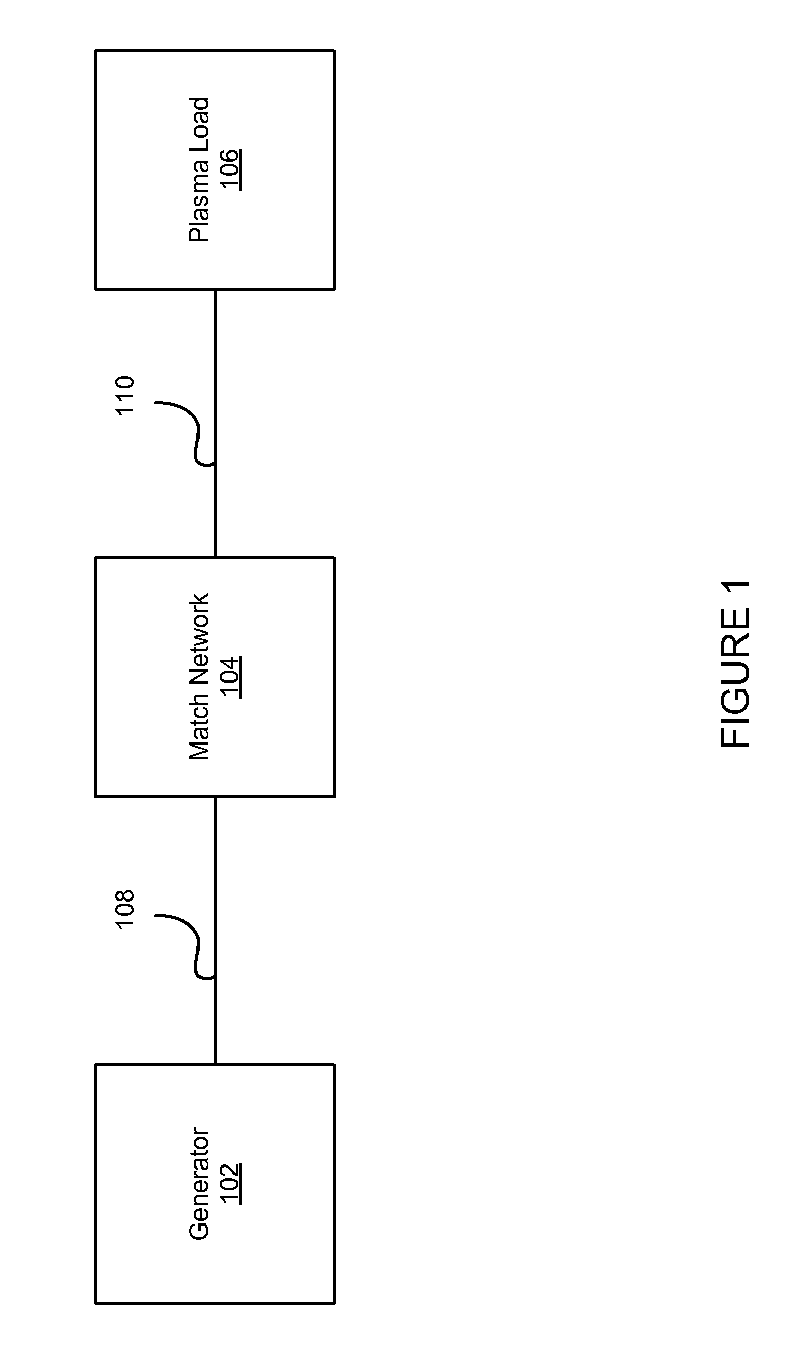
[0023]FIG. 1 is a circuit diagram of a plasma processing system according to one embodiment of this invention. A generator 102 transmits RF power to a match network 104 (“match”) via a transmission line 108 (e.g., coaxial cable) and then onto a plasma load 106 via an electrical connection 110. The match network 104 varies its internal electrical elements such that the input impedance of the match network 104 is close to the desired input impedance.

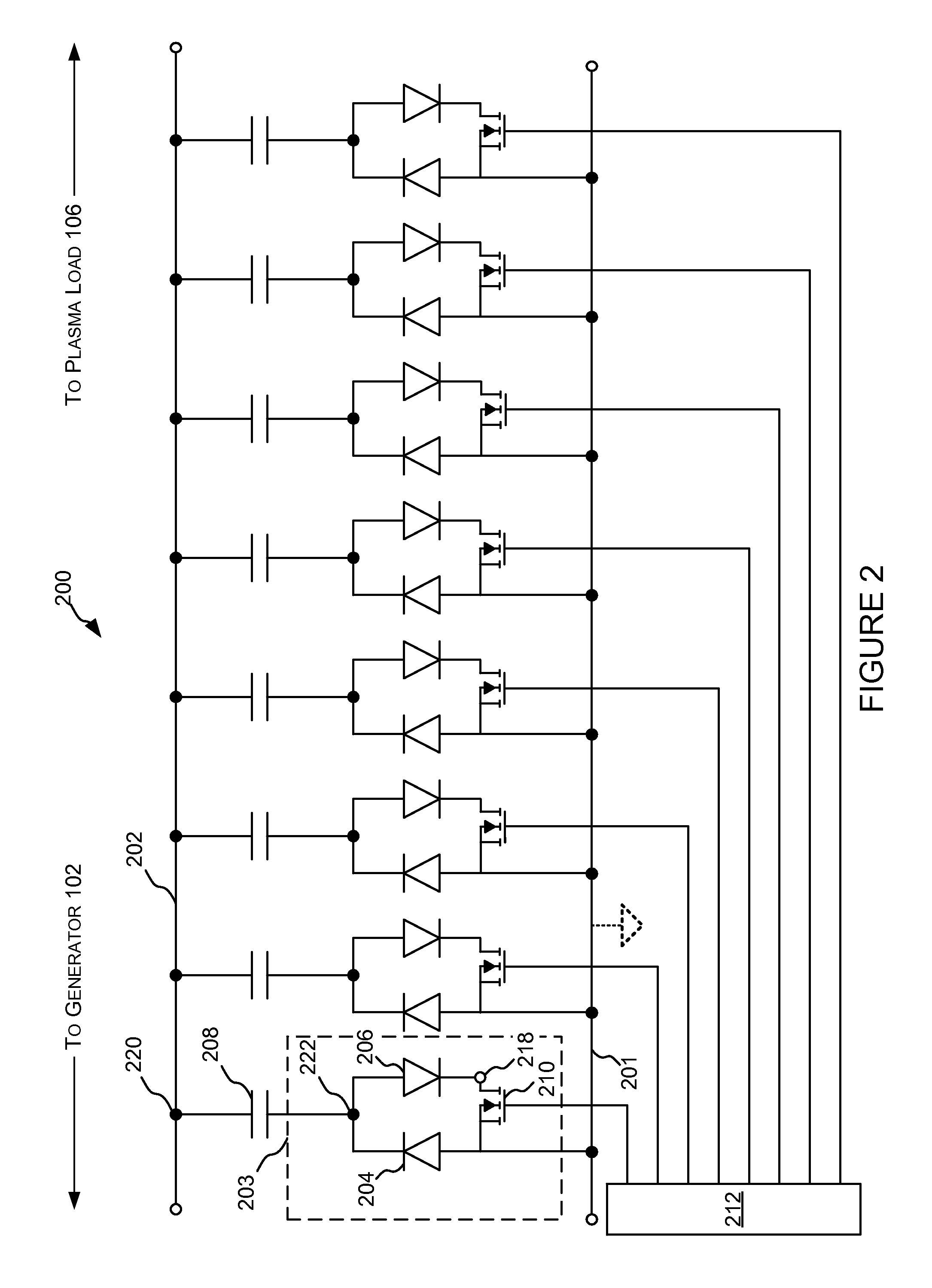
[0024]The match 104 can include two or more variable capacitance elements coupled in parallel. Often such variable capacitance elements can be mechanically-varied capacitors, which, as described above, are bulky, slow, and expensive. In the alternative, variable capacitive eleme...


PUM


Abstract

In accordance with this invention the above and other problems are solved by a switching apparatus and method that uses a switching circuit having a pair of parallel solid-state diodes (e.g., PN or PIN diodes), one of which is connected to a transistor (e.g., power MOSFET or IGBT), to switch a capacitor (or reactance element) in or out of a variable capacitance element (or variable reactance element) of an impedance matching network. Charging a body capacitance of the transistor reverse biases one of the two diodes so as to isolate the transistor from the RF signal enabling a low-cost high capacitance transistor to be used. Multiple such switching circuits and capacitors (or reactance elements) are connected in parallel to provide variable impedance for the purpose of impedance matching.

Description

CLAIM OF PRIORITY UNDER 35 U.S.C. §120[0001]The present Application for Patent is a Continuation-in-Part of patent application Ser. No. 13 / 288,712 entitled “HIGH FREQUENCY SOLID STATE SWITCHING FOR IMPEDANCE MATCHING” filed Nov. 3, 2011, pending, and assigned to the assignee hereof and hereby expressly incorporated by reference herein.FIELD OF THE DISCLOSURE[0002]The present invention relates generally to plasma processing. In particular, but not by way of limitation, the present invention relates to systems, methods and apparatuses for impedance-matching radio frequency power transmitted from a radio frequency generator to a plasma load in a semiconductor processing chamber.BACKGROUND[0003]In the semiconductor manufacturing world, manufacturers produce plasma processing chambers that utilize radio frequency (RF) power to generate a plasma. In order to achieve efficient power transfer between the RF generator (“generator”) and the plasma load, an impedance-matching network (“match”)...

Claims


Application Information

Patent Timeline
Patent Type & Authority Applications(United States)
IPC IPC(8): H03H11/28
CPCH01J37/32183H03H7/40H03H11/28H03K17/56H03K17/74H05H2001/4682H05H2242/26
Inventor MASON, CHRISTOPHER C.
Owner AES GLOBAL HLDG PTE LTD
Why Eureka
Try Eureka