Starting material and process for producing a sintered join

a technology of starting material and process, applied in the direction of metal layered products, solid-state devices, metal-working apparatus, etc., can solve the problems of thermal stress, failure of assembly, electrical and mechanical properties decrease, etc., and achieve the effect of crack formation in the event and crack formation

Inactive Publication Date: 2013-08-22
ROBERT BOSCH GMBH
View PDF7 Cites 20 Cited by
  • Summary
  • Abstract
  • Description
  • Claims
  • Application Information

AI Technical Summary

Benefits of technology

[0011]Elemental silicon and silicon dioxide have an extremely low coefficient of thermal expansion α (CTE) and have therefore been found to be particularly advantageous for, inter alia, reducing the coefficient of thermal expansion of the sintered bond. Even the addition of a small amount therefore advantageously enables a larger reduction in the coefficient of thermal expansion of the sintered bond than is the case for other additives to be achieved. In addition, elemental silicon and silicon dioxide advantageously have low Young's moduli, which can have an advantageous effect on the elasticity of the sintered bond. A reduction in the coefficient of thermal expansion of the sintered bond and the good elastic properties can in turn significantly reduce the thermomechanical stress between the sintered bond and the semiconductor component bonded thereto and thus the tendency for crack formation in the semiconductor component. Owing to the advantageous coefficients of expansion and Young's moduli of elemental silicon and silicon dioxide, a sintered bond composed of a starting material according to the invention can advantageously have a lower coefficient of expansion at the same or even a lower Young's modulus than a similar unfilled sintered bond, in particular one which has a correspondingly larger proportion of first particles instead of a proportion of second particles. In addition, the materials costs can advantageously be reduced by the use of elemental silicon and / or silicon dioxide. Basically, particles composed of elemental silicon and / or silicon dioxide are advantageously chemically inert during a thermal treatment of the starting material to form a sintered bond and are present in unchanged form within the metal matrix formed in a sintered bond which has been formed.
[0088]In an alternative possible variant of the process of the invention, the sintered bond is formed in vacuo and / or under a nitrogen atmosphere. Since in this case excess reducing agent cannot be burnt, a starting material in which the proportion of the organic or inorganic metal compound, in particular the metal compound to be reduced, present in the starting material is present in a stoichiometric ratio to the proportion of the reducing agent present in the starting material should be provided. During the thermal treatment, the reducing agent is accordingly completely consumed. In addition, the organic or inorganic metal compound is completely converted into the metallic form. In this process variant, join partners having a contact point which does not contain noble metal and is instead composed, for example, of copper can advantageously also be provided. This enables inexpensive electrical and / or electronic components also to be employed.

Problems solved by technology

Further thermal stress is caused by the use of such electrical or electronic appliances in places of operation having a temperature which is significantly above room temperature and may also change continually.
However, such bonding layers display, particularly at use temperatures close to the melting point, a decrease in electrical and mechanical properties which can lead to failure of the assembly.
However, lead-containing solder bonds are greatly restricted in respect of their permissible industrial applications by legal obligations for reasons of environmental protection.
Lead-free hard solders generally have a melting point above 200° C. However, when hard solder is used for producing a bonding layer, only few electrical or electronic components which can withstand the high temperatures during melting of the hard solders come into question as join partners.
However, when such sintered bonds are subjected to temperature changes, thermomechanical stresses and even crack formation in semiconductor components or even in the support substrate can occur.

Method used


Image

  • Starting material and process for producing a sintered join
  • Starting material and process for producing a sintered join
  • Starting material and process for producing a sintered join

Examples


first embodiment

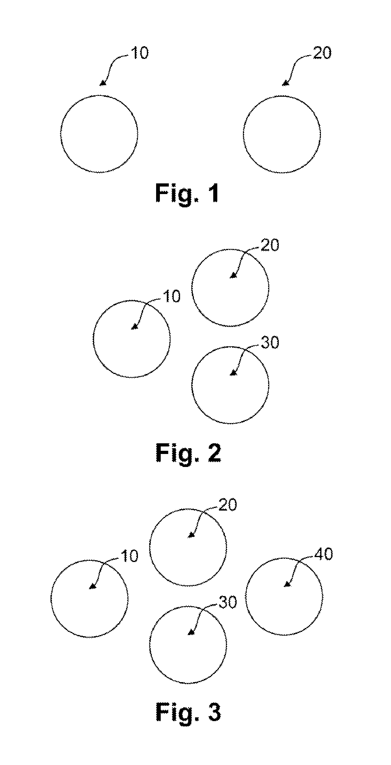
[0102]FIG. 1 schematically shows first particles 10 and second particles 20 which are provided in a starting material according to the invention for a sintered bond.

second embodiment

[0103]FIG. 2 schematically shows first particles 10, second particles 20 and third particles 30 which are provided in a starting material according to the invention for a sintered bond.

third embodiment

[0104]FIG. 3 schematically shows first particles 10, second particles 20, third particles 30 and fourth particles 40 which are provided in a starting material according to the invention for a sintered bond.

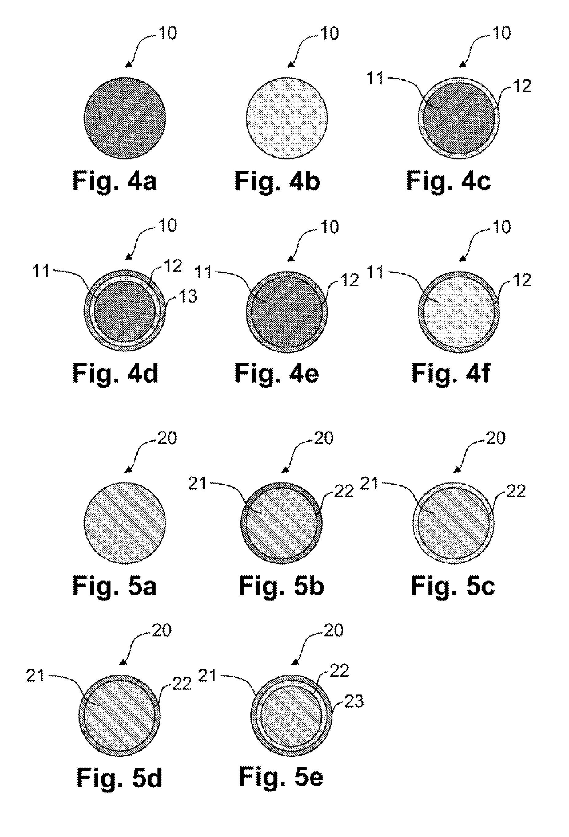
[0105]The starting material can, in the embodiments illustrated in FIGS. 1 to 3, contain metal-containing first particles 10 of one or more of the embodiments shown in FIGS. 4a to 4f. For example, the first particles 10 can be noble metal-containing and / or copper-containing, in particular silver-containing, particles. In the interests of simplicity, the figures are explained below for the example of silver-containing first particles 10. FIG. 4a shows a first particle 10 which is composed of silver in metallic form.

[0106]FIG. 4b shows a first particle 10 which is composed of an organic or inorganic silver compound, for example silver carbonate (Ag2CO3) and / or silver oxide (Ag2O, AgO), which can be converted into metallic silver by a thermal treatment.

[0107]FIG. 4c shows a first par...


PUM

PropertyMeasurementUnit
atmospheric humidityaaaaaaaaaa
humidityaaaaaaaaaa
temperature stressesaaaaaaaaaa

Abstract

The present invention relates to a starting material for producing a sintered join. In order to avoid the formation of cracks in the case of fluctuating thermal loading, the starting material comprises second particles 20, in addition to metallic first particles 10, which at least proportionately contain elemental silicon and / or silicon dioxide. In addition, the present invention relates to the use of elemental silicon and / or silicon dioxide for reducing the coefficient of thermal linear expansion α of a starting material 100 of a sintered join 100′ or of a sintered join 100′, in particular in a sintered paste, a sintered powder or a sintered material preform. Furthermore, the present invention relates to sintered joins 100′, to electronic circuits 70 and also to processes for forming a thermally and / or electrically conductive sintered join.

Description

BACKGROUND OF THE INVENTION[0001]The invention relates to a sintered bond, a starting material for producing it and a process for the production thereof, and also an electronic circuit containing the sintered bond.[0002]Power electronics are used in many fields of technology. Especially in electrical or electronic appliances in which large currents flow, the use of power electronics is indispensible. The currents necessary in power electronics lead to thermal stressing of the electrical or electronic components present therein. Further thermal stress is caused by the use of such electrical or electronic appliances in places of operation having a temperature which is significantly above room temperature and may also change continually. Examples which may be mentioned are control instruments in the automobile sector which are arranged directly in the engine compartment.[0003]In particular, many joins between power semiconductors or integrated circuits (ICs) among one another and also ...

Claims


Application Information

Patent Timeline
Patent Type & Authority Applications(United States)
IPC IPC(8): B23K35/24H05K1/02B32B15/04B22F1/18
CPCB22F1/02C22C32/0021H01B1/02H01L2224/8384H01L2224/29H01L2924/01006H01L2924/01021H01L2924/01037H01L2924/01055H01L2924/01074H01L2924/01078H01L2924/01079H01L2924/00013B23K35/0244H05K13/0465H01L2224/29439H01L2224/293H01L2224/29339H01L2224/29347H01L2224/29386H01L2224/294H01L2224/29486H01L2224/29469H01L2224/29464B23K35/24B32B15/043H05K1/0271Y10T403/477Y10T428/12069H01L2924/00014H01L2924/0541H01L2924/0461H01L2924/05442H01L2924/04642H01L2924/05032H01L2924/05042H01L2924/05432H01L2224/29099H01L2224/29199H01L2224/29299H01L2224/2929H01L2224/29311B22F1/18
Inventor KALICH, THOMASWOLDE-GIORGIS, DANIELFEIOCK, ANDREAKOLB, ROBERT
Owner ROBERT BOSCH GMBH
Why Eureka
Try Eureka