
Light emitting device material and light emitting device

a technology of light emitting device and material, which is applied in the direction of thermoelectric devices, triarylamine dyes, organic chemistry, etc., can solve the problems of insufficient luminance efficiency and device durable life, inability to achieve low driving voltage, and insufficient technology for achieving low driving voltage and durable life. , to achieve the effect of long lasting life, low driving voltage and high luminance efficiency

Inactive Publication Date: 2013-10-10
TORAY IND INC
View PDF2 Cites 7 Cited by
  • Summary
  • Abstract
  • Description
  • Claims
  • Application Information

AI Technical Summary

Benefits of technology

The present invention is about an organic thin-film light emitting device that has improved brightness and durability while keeping the driving voltage low. This device has high efficiency and can be used for a long time without being burned out.

Problems solved by technology

Conventional technologies were difficult to reduce the driving voltage of a device sufficiently, and even if they had been able to reduce the driving voltage, the luminance efficiency and the durable life of a device were insufficient.
Thus, technologies capable of realizing a low driving voltage, a high luminance efficiency, and a durable life have not been found, yet.

Method used


Image

  • Light emitting device material and light emitting device
  • Light emitting device material and light emitting device
  • Light emitting device material and light emitting device

Examples


synthesis example 1

Synthesis of Compound [71](HT-1)

[0090]A mixed solution of 20.9 g of 3,6-dibromophenylcarbazole, 15.0 g of phenylcarbazole-3-boronic acid, 366 mg of bis(triphenylphosphine) palladium (II) dichloride, 105 ml of a 1M aqueous sodium carbonate solution, and 260 ml of dimethoxyethane was refluxed for 5 hours under a nitrogen flow. After cooling to room temperature, extraction with toluene was conducted. The organic layer was washed with water twice, dried over magnesium sulfate, and evaporated. The resultant concentrate was purified by silica gel column chromatography and then vacuum-dried to obtain 13.5 g of 6-bromo-9,9′H-3,3′-bicarbazole.

[0091]Next, a mixed solution of 5.3 g of 6-bromo-9,9′H-3,3′-bicarbazole, 3.0 g of 4-(diphenylamino)phenylboronic acid, 66 mg of bis(triphenylphosphine)palladium (II) dichloride, 21 ml of a 1M aqueous sodium carbonate solution, and 47 ml of dimethoxyethane was refluxed for 5 hours under a nitrogen flow. After cooling to room temperature, water was poured...

example 1

[0095]A glass substrate with an ITO transparent electrically conductive film deposited thereon in a thickness of 165 nm (manufactured by GEOMATEC Co., Ltd., 11Ω / □, sputtered product) was cut into 38×46 mm, and then subjected to etching. The resulting substrate was ultrasound-washed with “SEMICOCLEAN 56” (trade name, manufactured by Furuuchi Chemical Corporation) for 15 minutes, and then washed with ultrapure water. This substrate was treated with UV-ozone for 1 hour immediately before manufacturing of a device, and placed in a vacuum evaporation apparatus, and the air was evacuated until the degree of vacuum in the apparatus was 5×10⁻⁴ Pa or lower. By a resistance heating method, HI-1 was evaporated as a hole injection layer in a thickness of 10 nm. Then, HT-1 was evaporated as a hole transporting layer in a thickness of 60 nm. Then, Compound H-1 and Compound D-1 were used as a host material and as a dopant material, respectively, and were evaporated as an emissive layer in a thickn...

examples 2 to 19

[0097]According to the same manner as in Example 1 except that materials described in Table 1 were used as a hole transporting layer, light emitting devices were manufactured and evaluated. The results are shown in Table 1. HT-2 to HT-19 are compounds shown below.


PUM


Abstract

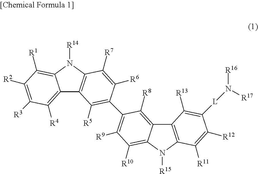
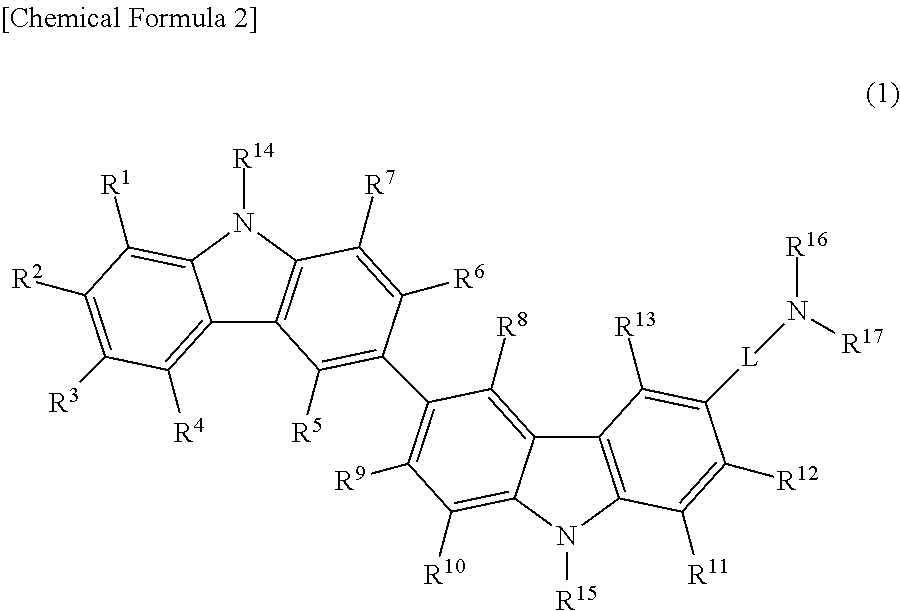
The present invention provides an organic thin-film light emitting device in which the luminance efficiency and durable life are improved while a low driving voltage is maintained by means of a light emitting device material that contains a compound represented by general formula (1).

Description

CROSS-REFERENCE TO RELATED APPLICATIONS[0001]This application is a U.S. National Phase Application of PCT International Application No. PCT / JP2011 / 079594, filed Dec. 21, 2011, which claims priority to Japanese Patent Application No. 2010-290139, filed Dec. 27, 2010, the contents of these applications being incorporated by reference herein in their entirety.FIELD OF INVENTION[0002]The present invention relates to a light emitting device capable of converting electric energy into light, and a light emitting device material to be used for the same. In particular, the present invention relates to a light emitting device capable of being used for areas such as display devices, flat-panel displays, backlight, lighting, interior design, labels, signboards, electrophotography machines, and light signal generators, and also to a light emitting device material to be used for the same.BACKGROUND OF THE INVENTION[0003]Researches on an organic thin-film light emitting device in which electrons i...

Claims


Application Information

Patent Timeline
IPC IPC(8): H01L51/00H01L51/50
CPCC07D209/86C09K2211/1029H01L51/0059H01L51/0072H01L51/5012C09B57/00C09B57/008H01L51/0061H01L51/5016C09K11/06H05B33/10C09K2211/1007C09K2211/1011C09K2211/1014C07D209/88H10K85/631H10K85/636H10K85/6572H10K50/11H10K2101/10H10K50/15
Inventor MATSUKI, SHINICHITANAKA, DAISAKUTOMINAGA, TSUYOSHI
Owner TORAY IND INC
Learn More