Check patentability & draft patents in minutes with Patsnap Eureka AI!

Super lattice structure, semiconductor device and semiconductor light emitting device having super lattice structure, and method of making super lattice structure

Inactive Publication Date: 2013-10-17
THE UNIV OF TOKYO +1
View PDF24 Cites 34 Cited by
  • Summary
  • Abstract
  • Description
  • Claims
  • Application Information

AI Technical Summary

Benefits of technology

The present invention provides a new method for producing a superlattice structure using multiply-stacked quantum dots on the same substrate. This method reduces the number of dislocations and defects, and improves the efficiency of semiconductor light emitting devices. The method ensures the uniform size of quantum-dot layers in the nanowires and minimizes the variation in quantum-dot layer size between nanowires. This results in improved strain and reduced power consumption.

Problems solved by technology

While the most popular photovoltaic elements now are single-junction solar cells using silicon, the silicon solar cells fail to absorb light in a longer wavelength range in the solar light spectra, and most of solar light energy has been not utilized.
However, the method of forming the quantum dots through the use of SK growth uses energy of lattice strain due to differences in lattice constant from substrate crystals (lattice mismatch), and the quantum-dot layer formed by SK growth is thus likely to be affected by the influence of strain, and becomes increasingly likely to be affected by the influence of strain with progression of stacking.
Therefore, the quantum-dot layer will become non-uniform as the layer is highly stacked.
In addition, the quantum-dot nanowire formed by the top-down approach such as an etching method is likely to be defective because strain is caused at the stage of thin film formation before the etching, and the influence of the strain may remain.
In particular, in the case of forming a highly-stacked quantum-dot nanowire, vertical etching is difficult because of anisotropy, and thus, the quantum-dot layer may vary in size, and produce remarkable non-uniformity.
Furthermore, while the quantum-dot nanowire formed by the bottom-up approach such as the VLS method is less likely to be affected by the influence of strain as compared with the quantum-dot nanowire formed by SK growth, there is a tendency to fail to keep the uniformity and undergo a decrease in diameter as the nanowire is highly stacked, and the quantum-dot layer may vary in size between the bottom and top thereof.
In addition, in the case of preparing a large number of quantum-dot nanowires, the respective quantum-dot nanowires are not necessarily uniform in properties such as diameter, verticality to the substrate, and size for each quantum-dot layer, and in particular, in the case of forming highly-stacked quantum-dot nanowires, this non-uniformity may be remarkably produced.
In addition, when, after the formation of quantum-well thin films, the strain thereof is used to stack quantum dots in a self-organizing manner, many dislocations and defects are caused, and there is thus possibility that the luminous efficiency will be decreased significantly.
In addition, it is generally not easy to control the sizes of the quantum dots prepared in a self-organizing manner, and multiply-stacked quantum dots of different sizes also have the possibility of making the preparation of quantum dots further difficult, also make it further difficult to control the sizes of quantum dots, and thus have the problem of failing to easily obtain desired emission spectra.

Method used


Image

  • Super lattice structure, semiconductor device and semiconductor light emitting device having super lattice structure, and method of making super lattice structure
  • Super lattice structure, semiconductor device and semiconductor light emitting device having super lattice structure, and method of making super lattice structure
  • Super lattice structure, semiconductor device and semiconductor light emitting device having super lattice structure, and method of making super lattice structure

Examples


first embodiment

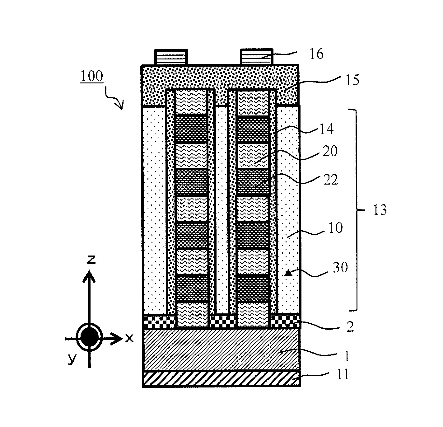
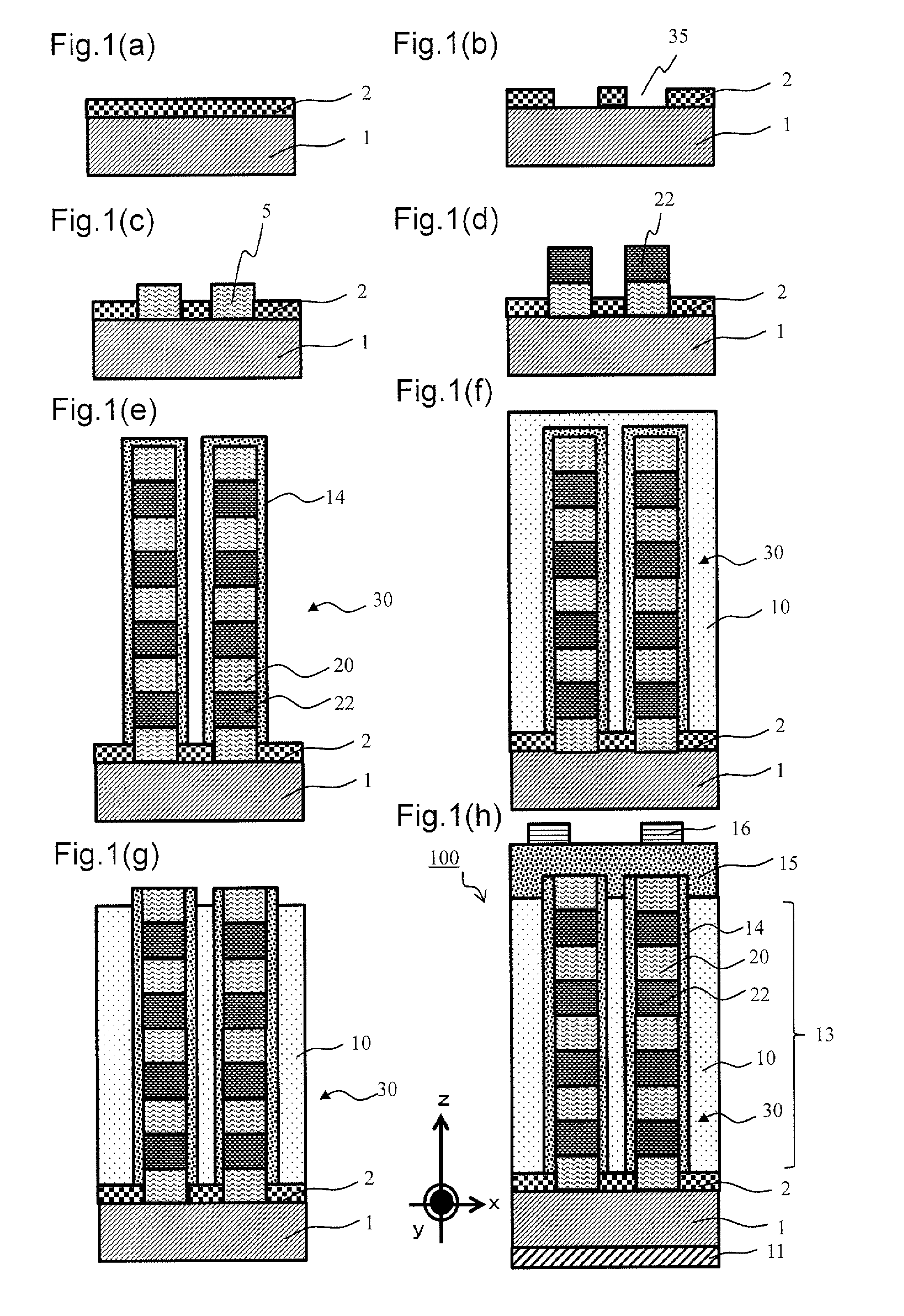
[0123]Next, a solar cell 100 according to a first embodiment will be described with reference to FIGS. 1A through 6.

[0124]It is to be noted that the following examples are by way of example, and respective materials such as substrates, buffer layers, quantum dots, dopants, electrodes for use in the solar cell 100 including the superlattice structure according to the present invention, cleaning agents, substrate treatment temperatures, manufacturing equipment for use in each process, etc. are not limited to the examples given herein. The same applies to other embodiments.

[0125]FIGS. 1A to 1H are diagrams illustrating a process for manufacturing a solar cell including a superlattice structure according to the first embodiment of the present invention.

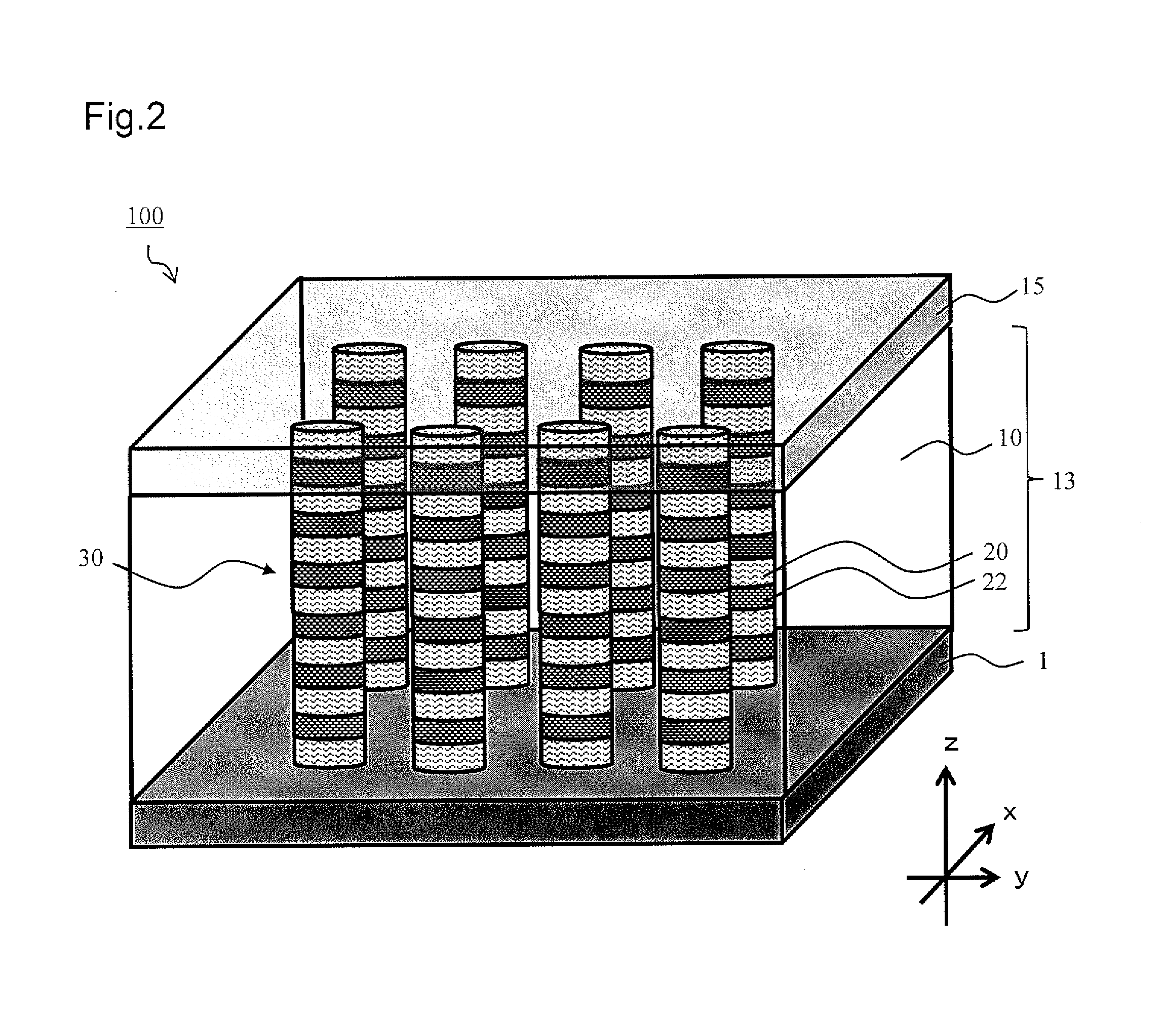
[0126]The solar cell 100 according to the first embodiment includes an n-type semiconductor layer 1, a p-type semiconductor layer 15, and a superlattice semiconductor layer 13 sandwiched between the n-type semiconductor layer 1 and the p-...

second embodiment

[0230]Next, a configuration of a solar cell 100b according to a second embodiment of the present invention will be described with reference to FIGS. 9A to 9H.

[0231]FIGS. 9A to 9H are diagrams illustrating a process for manufacturing a solar cell including a superlattice structure according to the second embodiment of the present invention.

[0232]As shown in FIGS. 9E to 9H, in the process for manufacturing the solar cell 100b, in a region in the x-y plane on the order of a solar light wavelength (for example, 500 nm) or less, further preferably in a region in the x-y plane on the order of a ultraviolet light wavelength (for example, 300 nm) or less, quantum-dot nanowires 30 and 30a of different types of diameters are formed, where quantum-dot layers 22 and 22a that are the same in size, material, and mixed crystal ratio are formed in the z direction.

[0233]As a specific manufacturing method, openings 35 and 35a of different diameters (sizes) are formed in advance in a mask layer 2 as s...

third embodiment

[0260]Next, a solar cell 100d including a superlattice semiconductor layer 13l according to a third embodiment of the present invention will be described with reference to FIGS. 13A to 13H.

[0261]FIGS. 13A to 13H are diagrams illustrating a process for manufacturing a solar cell including a superlattice structure according to the third embodiment of the present invention.

[0262]As shown in FIG. 13H, the solar cell 100d including quantum-dot nanowires has quantum-dot nanowires 30e arranged in an x-y in-plane region, where the quantum-dot nanowires 30e have quantum-dot layers 22 and 22b of the same diameter and different lengths in the z direction.

[0263]Specifically, as shown in FIGS. 13E to 13H, openings 35 in a mask layer 2 of SiO2 are made equal in size, and the quantum-dot layers 22 and 22b of different lengths are stacked in the stacking direction of the quantum-dot nanowires 30e. The use of this approach can change the quantum-dot layers in size intentionally in a controllable man...


PUM


Abstract

A superlattice structure includes a plurality of quantum-dot nanowires extending in a substantially vertical direction from a plane region. The quantum-dot nanowires have a structure of barrier layers and quantum-dot layers alternately stacked on the plane region, and the quantum-dot nanowires are substantially the same in diameter in a stacking direction and substantially uniformly arranged at an area density of 4 nanowires / μm2 or more.

Description

CROSS-REFERENCE TO RELATED APPLICATION[0001]This application relates to Japanese Patent Applications No. 2012-093240 filed on Apr. 16, 2012 and No. 2012-187856 filed on Aug. 28, 2012, whose priorities are claimed and the disclosures of which are incorporated by reference in their entirety.BACKGROUND OF THE INVENTION[0002]1. Field of the Invention[0003]The present invention relates to a superlattice structure, a semiconductor device and a semiconductor light emitting device including the superlattice structure, and a method for manufacturing the superlattice structure.[0004]2. Description of the Related Art[0005]In recent years, photovoltaic elements have been attracting attention as clean energy sources which emit no CO2, and becoming popular. While the most popular photovoltaic elements now are single-junction solar cells using silicon, the silicon solar cells fail to absorb light in a longer wavelength range in the solar light spectra, and most of solar light energy has been not u...

Claims


Application Information

Patent Timeline
IPC IPC(8): H01L33/04H01L29/15
CPCH01L33/04H01L33/06H01L29/15
Inventor NOZAWA, TOMOHIROARAKAWA, YASUHIKOTATEBAYASHI, JUN
Owner THE UNIV OF TOKYO
Features
  • R&D
  • Intellectual Property
  • Life Sciences
  • Materials
  • Tech Scout
  • Unparalleled Data Quality
  • Higher Quality Content
  • 60% Fewer Hallucinations
Learn More