Light-emitting device

a light-emitting device and color technology, applied in the direction of semiconductor devices, basic electric elements, electrical appliances, etc., can solve the problems of low current density of the carrier in the active layer, large active layer density, low application voltage, etc., to achieve high luminous efficacy and long life duration

Active Publication Date: 2013-10-17
SHIN-ETSU HANDOTAI CO LTD
View PDF0 Cites 20 Cited by
  • Summary
  • Abstract
  • Description
  • Claims
  • Application Information

AI Technical Summary

Benefits of technology

[0031]The configuration having the transparent films each having a large film thickness provided on the upper and lower sides of the active layer portion is a configuration that attaches a high value on light extraction from a lateral direction of a device rather than a vertical direction of the device. In this type of device, in case of reducing costs, decreasing a cross-sectional area of the device is effective, this means that a cross-sectional area in a current flowing direction is decreased, and the above-described configuration is a configuration that is suitable for a device in which a small current flows rather than a device in which a large current flows.

Problems solved by technology

However, since a bias difference is not large under such small-current conditions, a phenomenon that a first conductivity type carrier returns from a first conductivity type active layer to a cladding layer is a problem rather than an overflow phenomenon that the first conductivity type carrier injected into the active layer reaches a doped layer which is of a second conductivity type.
Since the carrier cannot sufficiently stay in the active layer due to occurrence of the phenomenon, a problem of a reduction in luminance arises.
However, these literatures are a countermeasure for the overflow of an n-type carrier from an active layer to a p-conductivity type layer, and it is restricted to a situation where current density of the active layer is large and an application voltage is high.
However, under small-current conditions, a large voltage that allows the n-type carrier to overflow to the p-conductivity type layer is not applied, and the current density of the carrier in the active layer is not high.
Therefore, the problem of the overflow in the device configuration used under the small-current conditions cannot be solved.

Method used


Image

  • Light-emitting device
  • Light-emitting device
  • Light-emitting device

Examples


examples

[0100]Although the present invention will now be more specifically explained based on examples and a comparative example hereinafter, the present invention is not restricted thereto.

examples 1 and 2

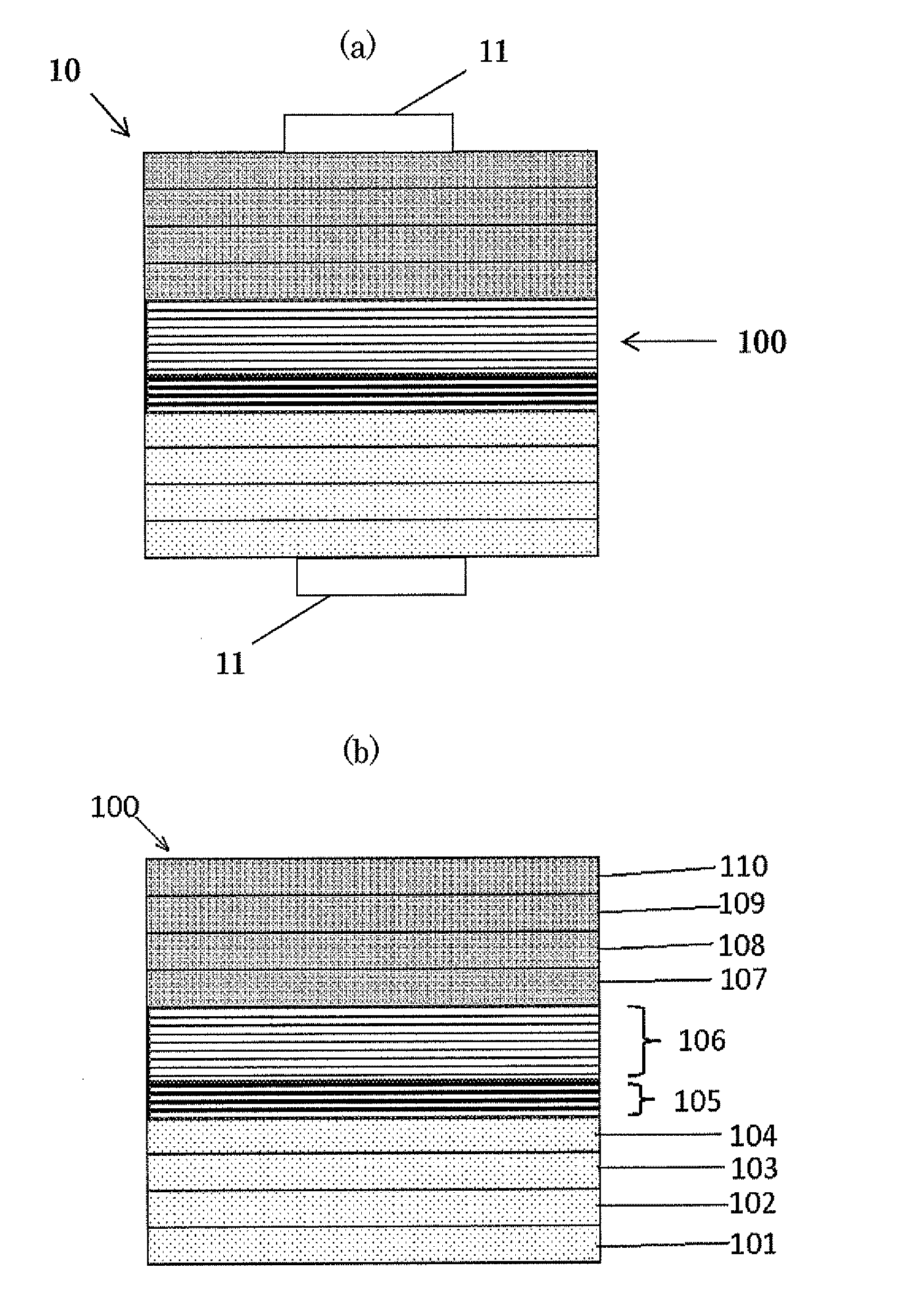
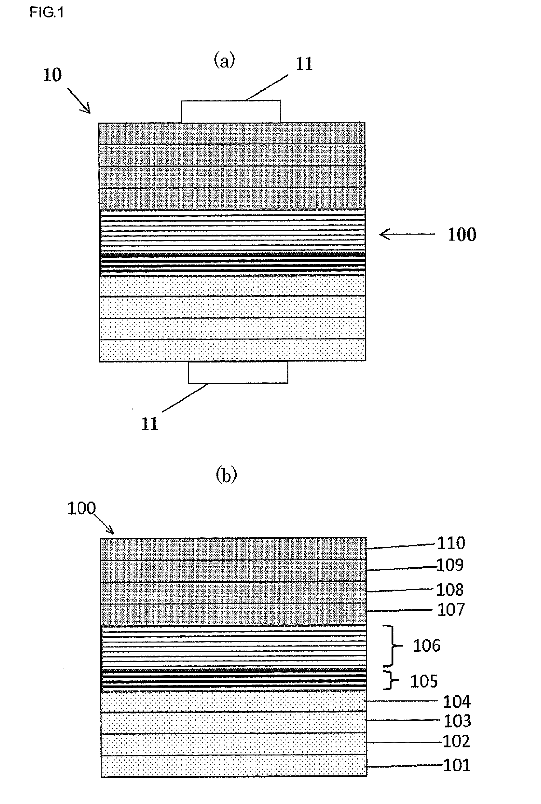
[0101]As Example 1, the light-emitting device 10 according to the first embodiment of the present invention shown in FIG. 1 was fabricated. Further, as Example 2, the light-emitting device 20 according to the second embodiment of the present invention shown in FIG. 6 was fabricated.

[0102]In each of Examples 1 and 2, a composition of the barrier layers 106E or 207B in the multiple-active layer portion 106 or 207 was Al0.85GaInP, and a composition of the barrier layers 106C or 207C was Al0.60GaInP. As a result, the band gap of the barrier layers on the side close to the p-type cladding layer was set smaller than that of the barrier layers on the side close to the n-type cladding layer.

[0103]Moreover, in each of Examples 1 and 2, each layer 105B or 205B was made of a material of a high-Al wide band gap layer (an AlInP layer) layer) low-Al narrow band gap layer (Al0.85GaInP) with a film thickness of 15 nm, each layer 105A or 205A was made of a material of a low-Al narrow band gap layer ...

examples 3 and 4

[0109]As Example 3, the light-emitting device 10 according to the first embodiment of the present invention shown in FIG. 1 was fabricated. Further, as Example 4, the light-emitting device 20 according to the second embodiment of the present invention shown in FIG. 6 was fabricated.

[0110]In each of Examples 3 and 4, a composition of the barrier layers 106B or 207B in the multiple-active layer portion 106 or 207 was Al0.85GaInP, and a composition of the barrier layers 106C or 207C was Al0.60GaInP. As a result, the band gap of the barrier layers on the side close to the p-type cladding layer was set smaller than that of the barrier layers on the side close to the n-type cladding layer.

[0111]Moreover, in each of Examples 3 and 4, each layer 105B or 205B was made of a material of a high-Al wide band gap layer (an AlInP layer) with a film thickness of 15 nm, each layer 105B or 205B was made of a material of a low-Al narrow band gap layer (a GaInP layer) with a film thickness of 15 nm, an...


PUM

PropertyMeasurementUnit
thicknessesaaaaaaaaaa
thicknessaaaaaaaaaa
thicknessaaaaaaaaaa

Abstract

The present invention provides a light-emitting device manufactured with use of a compound semiconductor substrate comprising at least: a p-type cladding layer; a multiple-active layer portion in which three or more active layers made of (AlxGa1-x)yIn1-yP (0≦x≦0.6, 0.4≦y≦0.6) and two or more barrier layers having a higher Al content rate x than the active layers are alternately laminated; and an n-type cladding layer, wherein the barrier layer on a side close to the p-type cladding layer has a smaller band gap than that of the barrier layer on a side close to the n-type cladding layer in the barrier layers, and the compound semiconductor substrate has a superlattice barrier layer between the multiple-active layer portion and the n-type cladding layer or in the n-type cladding layer. As a result, the light-emitting device having long life duration, low resistance, and high light-emitting efficiency (especially internal quantum efficiency) can be provided.

Description

BACKGROUND OF THE INVENTION[0001]1. Field of the Invention[0002]The present invention relates to a colored light-emitting device which can serve as an illumination or a light source for an indicator, and more particularly to a light-emitting device having multiple active layers.[0003]2. Description of the Related Art[0004]Since a light-emitting device having AlGaInP as a light-emitting layer is at least one digit brighter than a conventional colored light-emitting device, demands in use applications different from a conventional light-emitting diode, e.g., an in-car illumination or an LCD backlight are expanding. Although a fact that AlGaInP is of a direct transition type also contributes to an increase in intensity, enhancement of external quantum efficiency by providing a transparent and thick window layer is also a factor of the increase in intensity.[0005]On the other hand, for example, Non-patent Literature 1 discloses that internal quantum efficiency is enhanced by providing a...

Claims


Application Information

Patent Timeline
Patent Type & Authority Applications(United States)
IPC IPC(8): H01L33/14
CPCH01L33/145H01L33/06H01L33/30
Inventor ISHIZAKI, JUNYA
Owner SHIN-ETSU HANDOTAI CO LTD
Why Eureka
Try Eureka