Semiconductor device and manufacturing method therefor

a semiconductor and semiconductor technology, applied in the direction of semiconductor devices, electrical devices, transistors, etc., can solve the problems of dielectric and achieve the effects of preventing the breakdown of the gate insulating film caused by displacement current, reducing the resistance of the protective contact, and small resistance value between the protective diffusion layer and the base region

Active Publication Date: 2013-10-31
MITSUBISHI ELECTRIC CORP
View PDF3 Cites 37 Cited by
  • Summary
  • Abstract
  • Description
  • Claims
  • Application Information

AI Technical Summary

Benefits of technology

[0017]According to the present invention, since the protective contact that connects the protective diffusion layer and the source electrode is disposed on at least one of the blocks divided by the lattice-shaped gate electrode, an area of the protective contact that is as large as an area of the block can be secured. Therefore, the resistance of the protective contact can be lowered, and a resistance value between the protective diffusion layer and the base region can be small. Therefore, breakdown of the gate insulating fil

Problems solved by technology

At this time, a voltage drop occurs in a resistance component between the protective diffusion l

Method used


Image

  • Semiconductor device and manufacturing method therefor
  • Semiconductor device and manufacturing method therefor
  • Semiconductor device and manufacturing method therefor

Examples


first embodiment

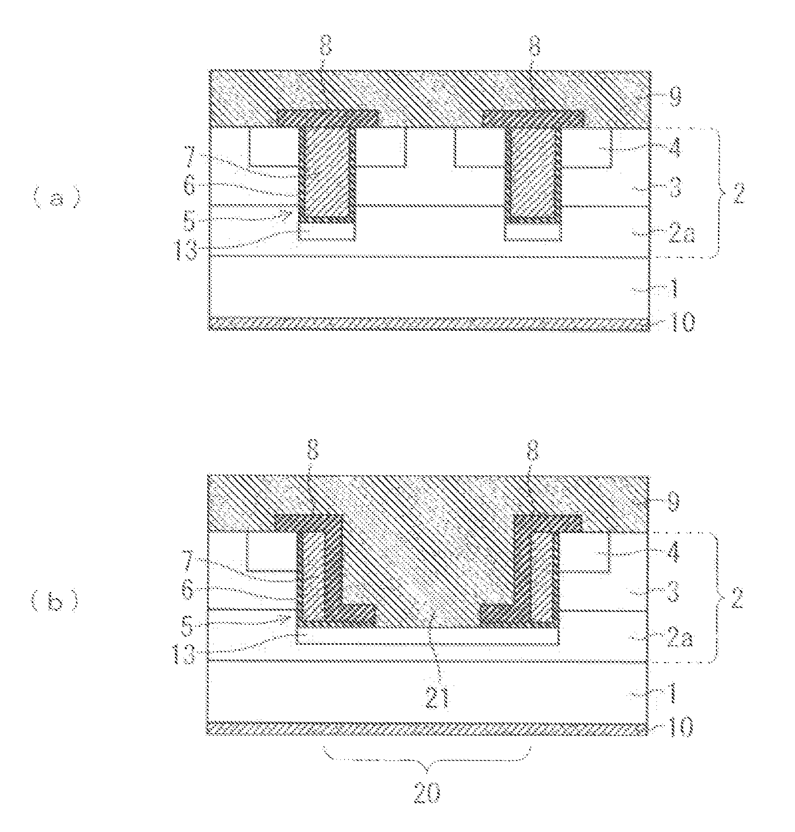
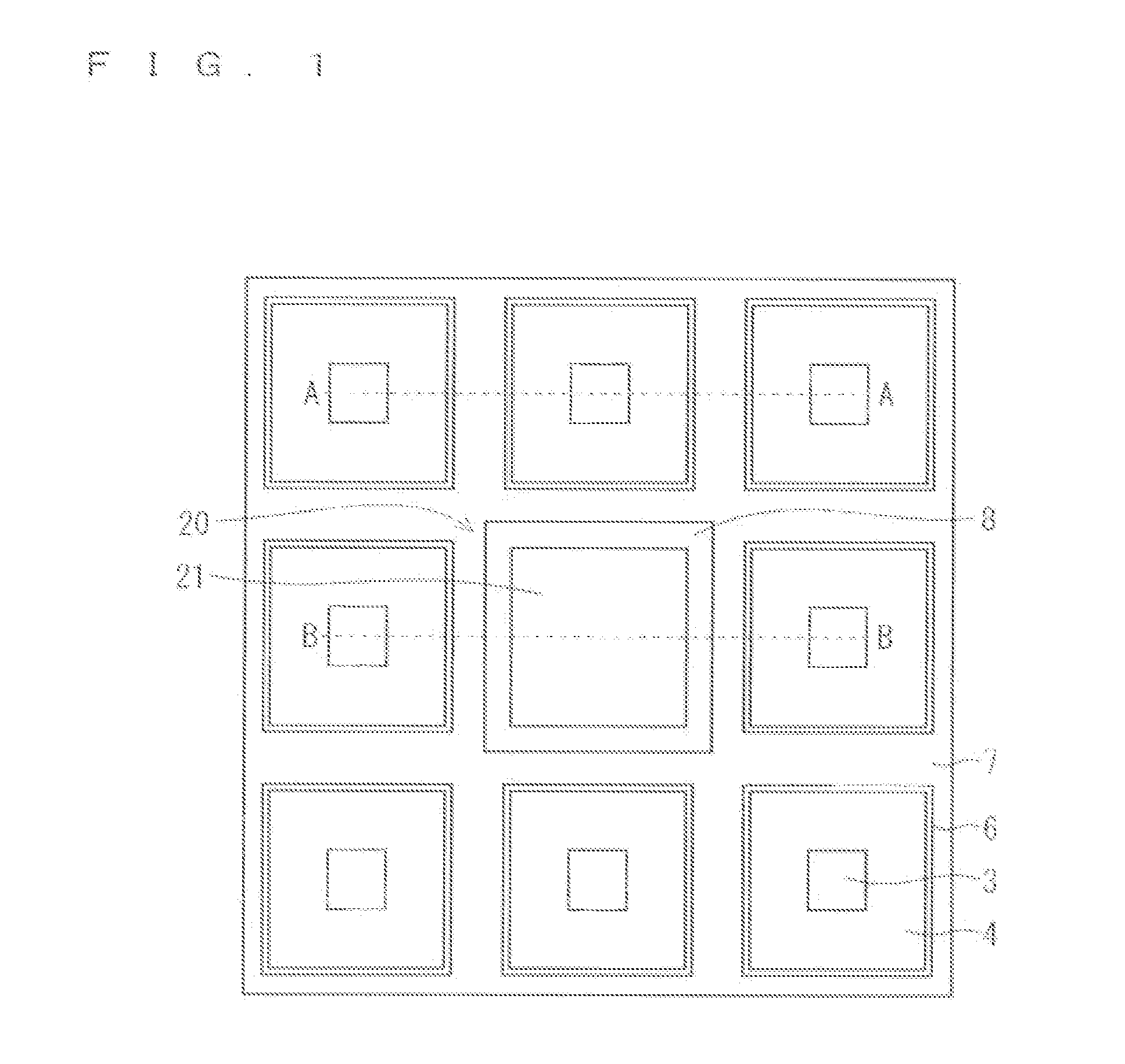
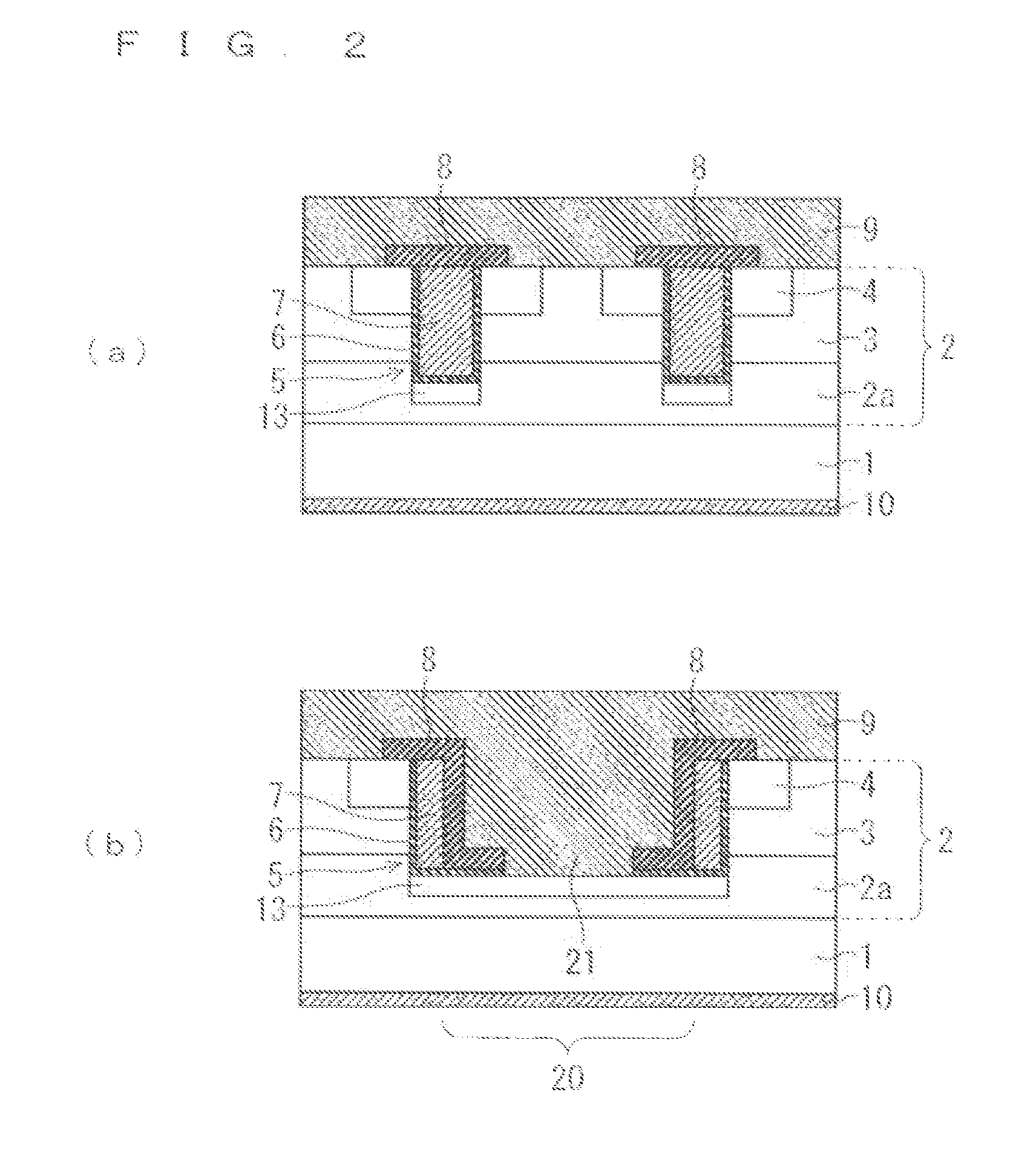
[0033]FIG. 1 and FIG. 2 are views each illustrating a configuration of a semiconductor device according to a first preferred embodiment. Here, a trench-gate type MOSFET is illustrated that is a silicon carbide (SiC) semiconductor device as one example of the semiconductor device. FIG. 1 is a plan view of the MOSFET. FIG. 2(a) is a sectional view taken along line A-A of FIG. 1, and illustrates a MOSFET cell forming region (MOSFET cell region). On the other hand, FIG. 2(b) is a sectional view taken along line B-B of FIG. 1, and includes a contact (protective contact) forming region 20 (protective contact region) to be connected to the protective diffusion layer. Details of the protective contact region 20 will be described later.

[0034]The MOSFET in the first preferred embodiment is formed by using an epitaxial substrate composed of an n-type SiC substrate 1 and an epitaxial layer 2 (semiconductor layer) of n-type SiC grown thereon. A p-type base region 3 is formed in the upper part of...

second embodiment

[0067]As described in the first preferred embodiment, the gate electrode 7 can be formed by any one of the patterning and etchback methods. However, when the trench 5 of the protective contact region 20 is formed into a tapered shape and the gate electrode 7 is tried to be formed by etchback, the gate electrode 7 disposed in the trench 5 of the protective contact region 20 might be completely removed.

[0068]The above problem is solved by forming the gate electrode 7 through the patterning. However, in this case, since the end of the gate electrode 7 is positioned on the upper surface of the epitaxial layer 2, the width of the gate electrode 7 becomes wider than the width of the trench 5. Therefore, from a viewpoint of narrowing of the pitch of the MOSFET cells, it is advantageous to obtain the gate electrode 7 through etchback.

[0069]In the second preferred embodiment, therefore, only the gate electrode 7 disposed in the trench 5 of the protective contact region 20 is formed by patter...

third embodiment

[0074]FIG. 13 is a sectional view illustrating the configuration of the semiconductor device according to the third preferred embodiment of the present invention, and illustrates a cross section of an outermost peripheral portion of a MOSFET cell array of the semiconductor device. In this preferred embodiment, a dummy cell 30 that does not function as a MOSFET is disposed so as to be adjacent on an outer side of the outermost peripheral MOSFET cells. The dummy cells 30 are arranged so as to surround the MOSFET cell array. A configuration of the MOSFET cell array (including the protective contact region 20) other than the outermost peripheral portion is similar to that in the first or second preferred embodiment.

[0075]As shown in FIG. 13, the dummy cell 30 has the trench 5 that penetrates the base region 3 similarly to the MOSFET cells, but the inside of the trench 5 is filled with a part of a field insulating film 22 to be formed on an outer peripheral region of the semiconductor de...


PUM


Abstract

A trench-gate type semiconductor device that can prevent breakdown of a gate insulating film caused by a displacement current flowing into a protective diffusion layer at a portion of a trench underlying a gate electrode at a turn-off time and simultaneously improves a current density by narrowing a cell pitch. The semiconductor device includes a gate electrode embedded into a trench penetrating a base region. The gate electrode is disposed into a lattice shape in a planar view, and a protective diffusion layer is formed in a drift layer at the portion underlying thereof. At least one of blocks divided by the gate electrode is a protective contact region on which the trench is entirely formed. A protective contact for connecting the protective diffusion layer at a bottom portion of the trench and a source electrode is disposed on the protective contact region.

Description

TECHNICAL FIELD[0001]The present invention relates to a trench-gate type semiconductor device and a manufacturing method therefor.BACKGROUND ART[0002]In power electronics devices, as switching elements for controlling power supply to loads such as motors, insulating gate type semiconductor devices, such as an IGBT (Insulated Gate Bipolar Transistor) and a MOSFET (Metal Oxide Semiconductor Field Effect Transistor), are widely used. As one of vertical MOSFETs for power control, there is a trench-gate type MOSFET in which a gate electrode is embedded into a semiconductor layer (for example, the following Patent Documents 1 and 2). In general, in a trench-gate type MOSFET, heightening of withstand voltage and lowering of on resistance establish a trade-off relationship.[0003]On the other hand, an attention is paid to a MOSFET and an IGBT using a wide band gap semiconductor of silicon carbide (SiC) or the like as next-generation switching elements that can implement high withstand voltag...

Claims


Application Information

Patent Timeline
IPC IPC(8): H01L29/78H01L29/66
CPCH01L29/7827H01L29/66666H01L29/0623H01L29/0696H01L29/1608H01L29/2003H01L29/41766H01L29/42376H01L29/4238H01L29/66068H01L29/66348H01L29/66727H01L29/66734H01L29/7397H01L29/7811H01L29/7813H01L29/063H01L29/1095H01L29/1045H01L29/105H01L29/41741H01L29/41775H01L29/4236H01L29/6631H01L29/66522
Inventor KAGAWA, YASUHIROFURUKAWA, AKIHIKOHINO, SHIROWATANABE, HIROSHIIMAIZUMI, MASAYUKI
Owner MITSUBISHI ELECTRIC CORP
Why Eureka
Try Eureka