Flexible organic electroluminescent device and manufacturing method thereof

a flexible, organic technology, applied in the direction of thermoelectric device junction materials, semiconductor devices, electrical apparatus, etc., can solve the problems of oled application impact, many insurmountable problems, carrier and transmission performance uncontrollable, etc., to achieve good light transmission, simple manufacturing method, and less destructive effect of substra

Inactive Publication Date: 2013-11-21
OCEANS KING LIGHTING SCI&TECH CO LTD
View PDF3 Cites 4 Cited by
  • Summary
  • Abstract
  • Description
  • Claims
  • Application Information

AI Technical Summary

Benefits of technology

[0021]By adopting vacuum coating technology, ZnS / Ag / MoO3 multilayer composite structure is prepared as anode layer, and its manufacturing method is simple, less destructive to the substrate. In addition, the anode layer has good transmission of light and low surface resistance. Moreover, the bonding force between the anode layer and the substrate is enhanced by inserting buffer layer, so that the prepared flexible organic electroluminescent device has a good bending endurance performance, a stable luminous property and a high light emitting efficiency.

Problems solved by technology

The prior art OLED device provided with glass substrate does not have a curved features and the glass is fragile , thus impacting on the application of OLED.
However, there are many insurmountable problems existing in application of such conductive thin films in flexible OLED.
For example, in the process of manufacturing ITO thin film, the doping proportion of various elements, such as indium (In) and stannum (Sn), is difficult to control, resulting in uncontrollable morphology of ITO, carrier and transmission performance.
Therefore, performance of light-emitting device is unstable.
Secondly, when conductive thin film such as ITO is manufactured on flexible substrate, due to the poor heat resistance of the polymer thin film, low-temperature sputtering technique is usually adopted to prepare conductive thin film.
The conductive thin film as prepared has high surface resistance, weak bonding force between the thin film and the substrate, so that the conductive thin film is prone to fall off the substrate in the process of repeated bending, thus affecting the stability of the OLED device.

Method used


Image

  • Flexible organic electroluminescent device and manufacturing method thereof
  • Flexible organic electroluminescent device and manufacturing method thereof
  • Flexible organic electroluminescent device and manufacturing method thereof

Examples


example 1

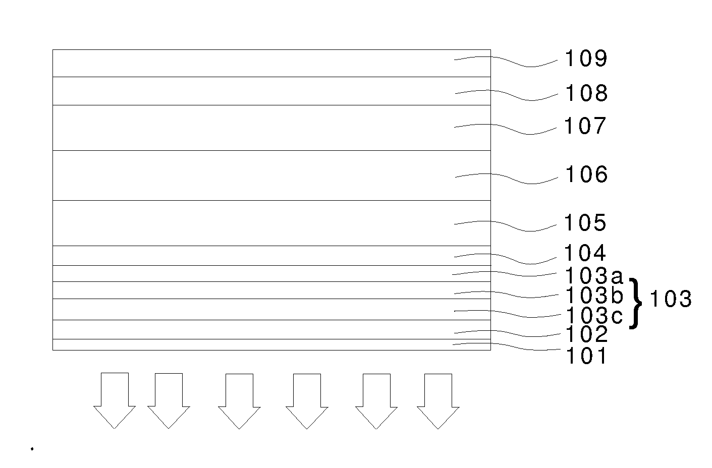
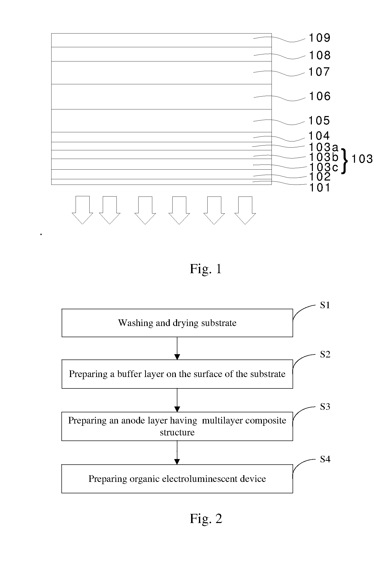
[0046]A flexible organic electroluminescent device, having layered structure as follows:

[0047]PET / UV glue / ZnS / Ag / MoO3 / m-MTDATA / NPB / Ir(ppy)3:CBP / TPBi / LiF / Mg—Ag.

[0048]The method for manufacturing the flexible electroluminescent device, comprising:

[0049]firstly, PEN film having a thickness of 0.1 mm was placed into deionized water containing detergent for ultrasonic cleaning, washed with deionized water, after that, ultrasonically treated successively with isopropanol and acetone, then blow dried with nitrogen;

[0050]then, the PEN film was placed on a spin coater, after starting the spin coater at a rotate speed of 1000 r / min, a layer of UV glue having a thickness of 0.5 μm was spin-coated on the PEN film as a flat layer, after 120 s, a UV lamp was employed to cure to form a buffer layer;

[0051]subsequently, in the coating system in a vacuum degree of 5×10⁻⁴Pa, ZnS layer having a thickness of 35 nm, Ag layer having a thickness of 18 nm, MoO3 layer having a thickness of 10 nm were vapor ...

example 2

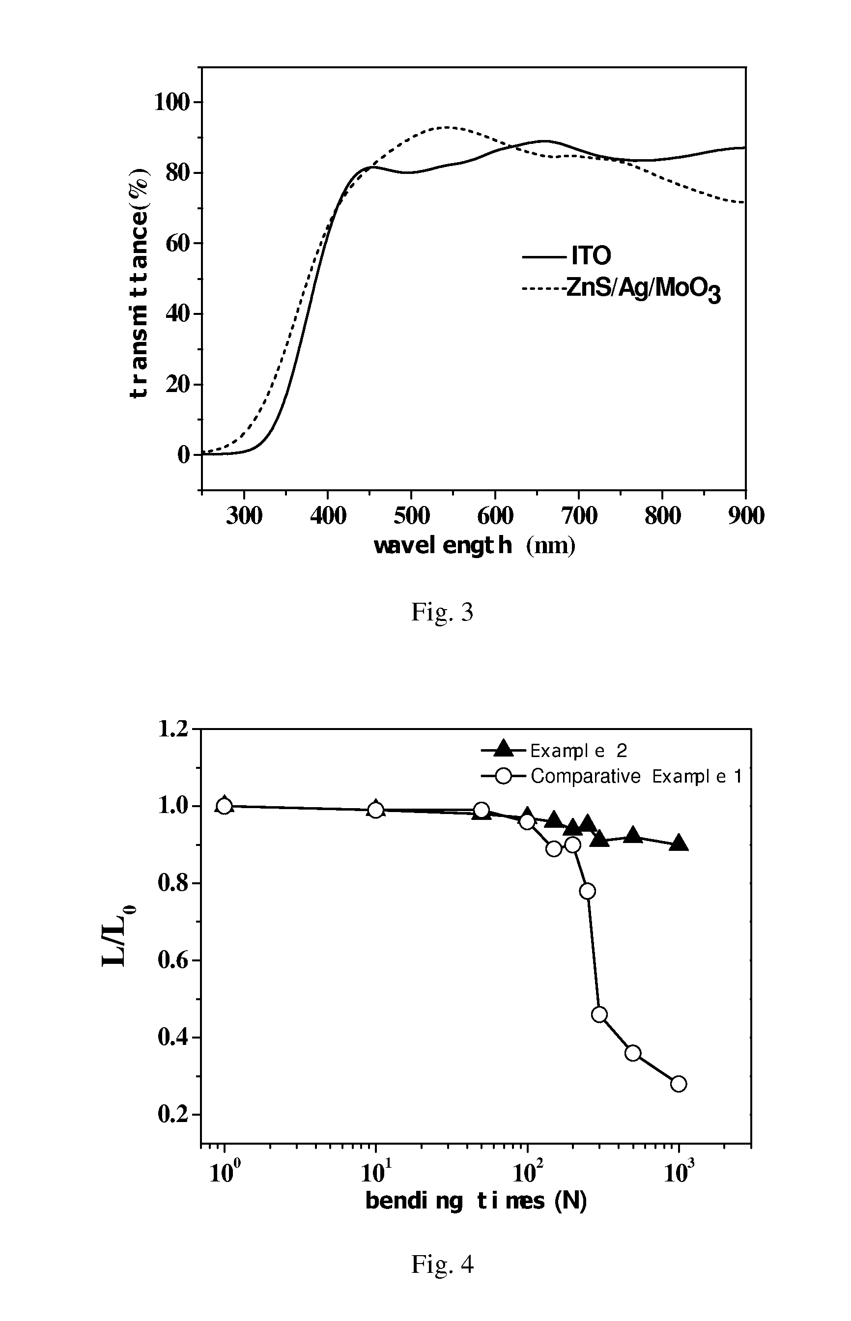
[0053]A flexible organic electroluminescent device, having layered structure as follows: PET / UV glue / ZnS / Ag / MoO3 / CuPc / TPD / DCJTB:Alq3 / Bphen / CsF / Ag.

[0054]The method for manufacturing the flexible electroluminescent device, comprising:

[0055]firstly, PET film having a thickness of 0.175 mm was placed into deionized water containing detergent for ultrasonic cleaning, washed with deionized water, after that, ultrasonically treated successively with isopropanol and acetone, then blow dried with nitrogen;

[0056]then, the PET film was placed on a spin coater, after starting the spin coater at a rotate speed of 5000 r / min, a layer of UV glue having a thickness of 5 μm was spin-coated on the PEN film as a flat layer, after 30 s, a UV lamp was employed to cure to form a buffer layer;

[0057]subsequently, in the coating system in a vacuum degree of 5×10⁻⁴Pa, ZnS layer having a thickness of 45 nm, Ag layer having a thickness of 20 nm, MoO3 layer having a thickness of 5 nm were vapor deposited succes...

example 3

[0059]A flexible organic electroluminescent device, having layered structure as follows: PES / UV glue / ZnS / Ag / MoO3 / m-MTDATA / TDAPB / α-NPD:Ir(MDQ)2(acac) / Alq3 / LiF / Al.

[0060]The method for manufacturing the flexible electroluminescent device, comprising:

[0061]firstly, PES film having a thickness of 0.2 mm was placed into deionized water containing detergent for ultrasonic cleaning, washed with deionized water, after that, ultrasonically treated successively with isopropanol and acetone, then blow dried with nitrogen;

[0062]then, the PES film was placed on a spin coater, after starting the spin coater at a rotate speed of 4000 r / min, a layer of UV glue having a thickness of 1 μm was spin-coated on the PEN film as a flat layer, after 70 s, a UV lamp was employed to cure to form a buffer layer;

[0063]subsequently, in the coating system in a vacuum degree of 5×10⁻⁴Pa, ZnS layer having a thickness of 80 nm, Ag layer having a thickness of 30 nm, MoO3 layer having a thickness of 3 nm were vapor dep...


PUM


Abstract

A flexible organic electroluminescent device and a manufacturing method thereof are provided. The device comprises a substrate (101), an anode layer (103), a hole-injecting layer (104), a hole-transporting layer (105), a light-emitting layer (106), an electron-transporting layer (107), an electron-injecting layer (108), and a cathode layer (109), which are stacked in order. The device further comprises a buffer layer (102) between the substrate (101) and the anode layer (103). The anode layer (103) is a multilayer composite structure, which comprises ZnS/Ag/MoO3. The bonding force between the anode layer (103) and the substrate (101) is enhanced by inserting buffer layer (102). The device has a good bending endurance performance, a stable luminous property and a high light emitting efficiency.

Description

FIELD OF THE INVENTION[0001]The present invention relates to the field of optoelectronic devices, and particularly relates to a flexible organic electroluminescent device. The present invention also relates to a method for manufacturing the flexible organic electroluminescent device.BACKGROUND OF THE INVENTION[0002]Organic electroluminescent device (Organic Light Emission Diode), hereinafter referred to as OLED, has characteristics such as high luminance, wide selection of material, low driving voltage and solid-state self-luminosity, as well as advantages such as high definition, wide viewing angle and fast response, which makes it not only conform to the development trends of mobile communication and information display in the information age, but also meet the requirements of green lighting technology. OLED is the primary focus of many domestic and overseas researchers.[0003]The prior art OLED device provided with glass substrate does not have a curved features and the glass is f...

Claims


Application Information

Patent Timeline
Patent Type & Authority Applications(United States)
IPC IPC(8): H01L51/52H01L51/56
CPCH01L51/5215H01L51/56H10K85/6572H10K77/111H10K50/816H10K2102/311H10K71/00
Inventor ZHOU, MINGJIEWANG, PINGFENG, XIAOMINGHUANG, HUI
Owner OCEANS KING LIGHTING SCI&TECH CO LTD
Why Eureka
Try Eureka