
Tunable semiconductor laser device and method for operating a tunable semiconductor laser device

a laser device and semiconductor technology, applied in semiconductor lasers, laser details, electrical devices, etc., can solve the problems of laser loss coupling, laser generated laser light will be doppler shifted, etc., to achieve different periodicities, prevent loss coupling, and widen the tuning range

Inactive Publication Date: 2013-11-21
EUPHOENIX
View PDF14 Cites 2 Cited by
  • Summary
  • Abstract
  • Description
  • Claims
  • Application Information

AI Technical Summary

Benefits of technology

The invention provides a design for a semiconductor laser that places the IDT (integrated double-sided thermal) in a way that prevents loss-coupling and the formation of a standing acoustic wave. This design also allows the IDT to create optical feedback in the entire active region, resulting in an acoustically induced Distributed Feedback (DFB) laser rather than an acoustically inducedDBR laser. The first and second IDTs can be placed symmetrically with respect to the central longitudinal structure, allowing the combined SAW to be located on or beneath the active region. This design prevents the need for high-quality optical feedback at the ends of the active region and improves the overall performance of semiconductor lasers.

Problems solved by technology

This design requires multiple sections in the laser diode and the traveling SAW is susceptible to damping, therefore requiring higher power or power controlling measures like reflectors and absorbers.
Another drawback of the ADBR design is that the generated laser light will be Doppler shifted since the light reflects off a traveling SAW.
It is also to be expected that the periodic metal lines of the IDT, placed directly above the path of the laser beam, may induce a loss-coupling in the laser.

Method used


Image

  • Tunable semiconductor laser device and method for operating a tunable semiconductor laser device
  • Tunable semiconductor laser device and method for operating a tunable semiconductor laser device
  • Tunable semiconductor laser device and method for operating a tunable semiconductor laser device

Examples


Embodiment Construction

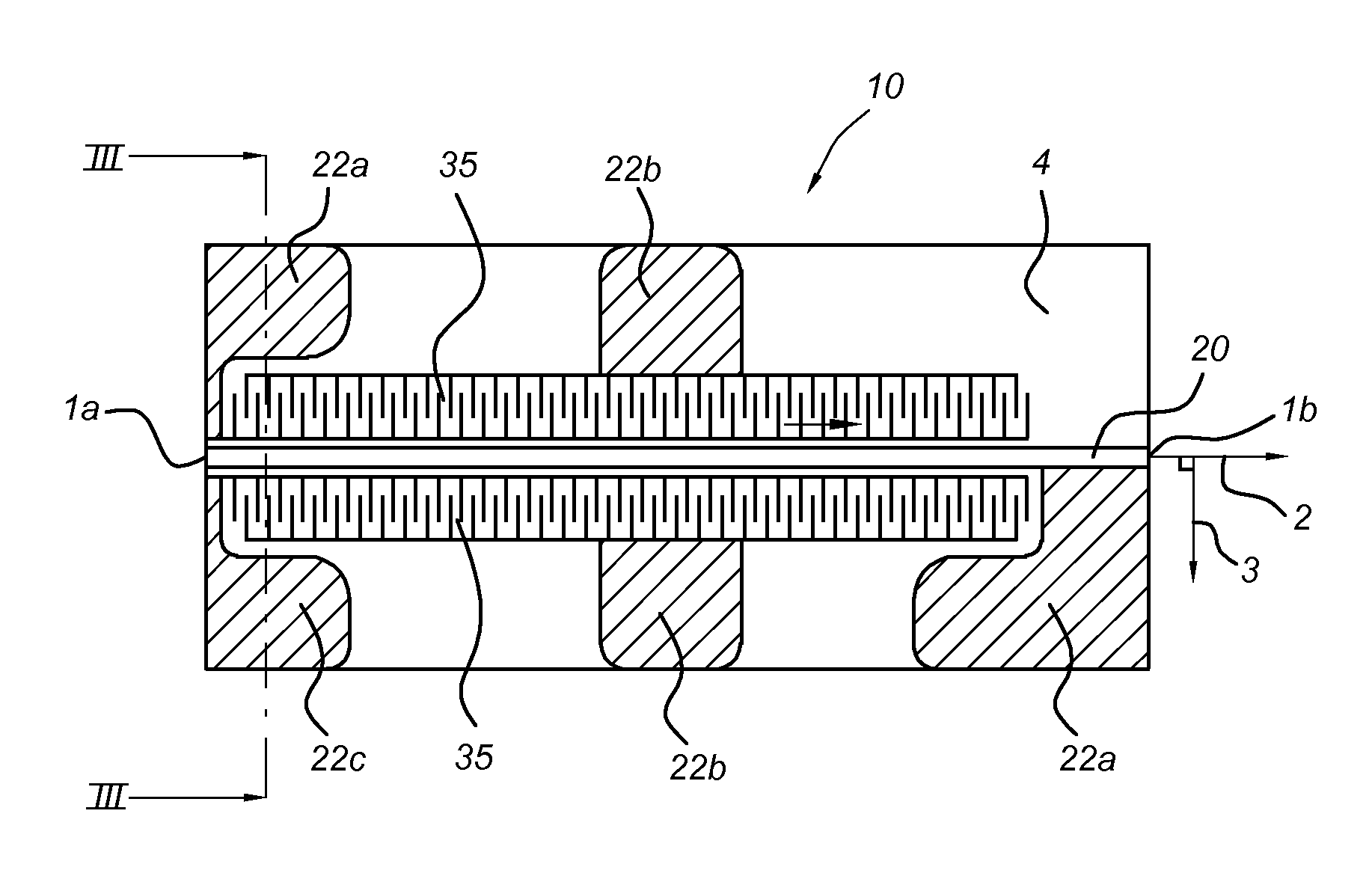
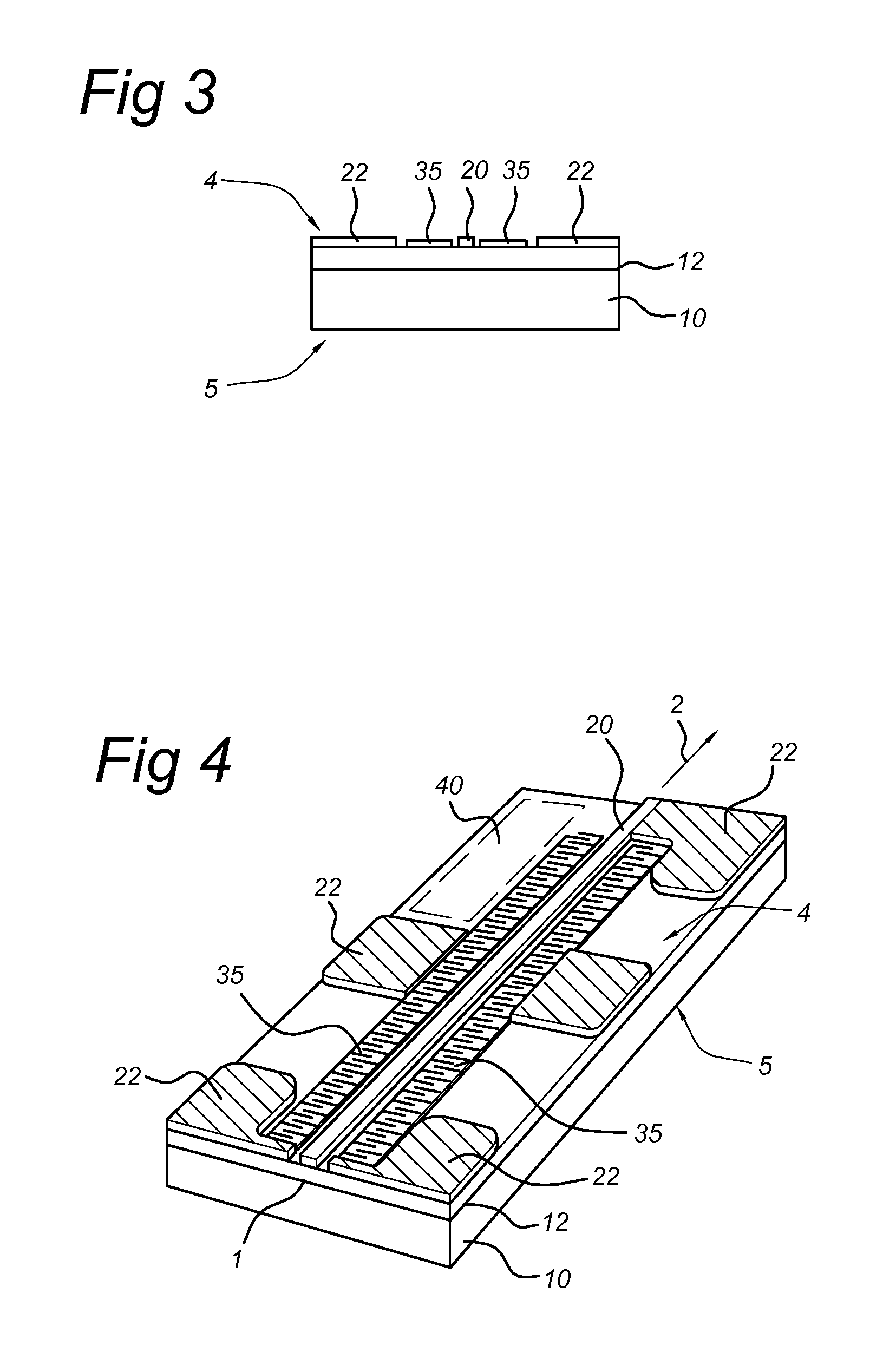
[0053]FIGS. 2, 3, and 4 schematically show respectively a top view, a side view, and a perspective view of a tunable semiconductor laser 10 according to an embodiment of the invention. The laser 10 comprises a diode structure having a p-n junction. In an example embodiment, the p-n junction is a III-V junction. Semiconductor lasers as such are known. Example laser diode designs are quantum cascade lasers, (separate confinement heterostructure), quantum well lasers, double heterostructure lasers, etc. Example materials for the diode structure are gallium arsenide (GaAs), indium phosphate (InP), gallium antimonide (GaSb), and gallium nitride (GaN) or mixtures of these, like InxGa1-xAlyAs1-y. It will be understood, however, by a person skilled in the art that other suitable materials exist and may be applied according the invention.

[0054]The laser 10 has a top surface 4 and a bottom surface 5, with an active layer 12 between the top and bottom surfaces. As described in the introduction...


PUM


Abstract

A tunable semiconductor laser device includes a semiconductor structure, a longitudinal structure provided on the top surface of the semiconductor structure, a first longitudinal interdigitated transducer, wherein the first IDT is arranged on one lateral side of the longitudinal structure and at a distance along the lateral axis from said structure and parallel to the longitudinal structure.

Description

FIELD OF THE INVENTION[0001]The invention relates to a tunable semiconductor laser device comprising a surface acoustic wave (SAW) resonator. In particular, the invention relates to such a device comprising an interdigitated transducer (IDT). The invention further relates to the use of such a tunable semiconductor laser device.BACKGROUND OF THE INVENTION[0002]Semiconductor laser devices, such as for example laser diodes, can be formed from semiconductor material, for example III-V material, with a p-n junction. Various structures are known to a skilled person. The earliest designs are homostructure lasers having a single p-n junction. More modern designs such as the double heterostructure (DH) laser diodes have a layer with a narrow energy bandgap sandwiched between two layers of a wider energy bandgap semiconductor. In general, the two heterojunctions help to confine the carriers in the central layer, which is usually called the active layer. The layers surrounding the central laye...

Claims


Application Information

Patent Timeline
Patent Type & Authority Applications(United States)
IPC IPC(8): H01S5/06
CPCH01S5/06H01S5/0607H01S5/1234H01S5/1237H01S5/22
Inventor ENGELMANN, MICHAELVAN-SOMEREN, BOB
Owner EUPHOENIX
Learn More