Sense amplifier circuitry for resistive type memory

a technology of resistive type memory and sense amplifier, which is applied in the direction of information storage, static storage, digital storage, etc., can solve the problems of voltage headroom problems in conventional sense amplifier circuitry, disadvantages in sense amplifier operation, and the lik

Active Publication Date: 2013-12-05
SAMSUNG ELECTRONICS CO LTD
View PDF1 Cites 29 Cited by
  • Summary
  • Abstract
  • Description
  • Claims
  • Application Information

AI Technical Summary

Problems solved by technology

Conventional sense amplifier technology used in resistive type memories can experience problems as the power supply voltages are decreasing over time.
Whereas in times past the power supply voltage for a memory circuit may have been 5 Volts (V) or 3.3 V, for example, today a power supply voltage may supply voltages around 1.2 V or 1.3 V. Such low power supply voltages can cause voltage headroom problems in conventional sense amplifier circuitry as the saturation voltage of a transistor may not scale down proportionally to the supply voltage.
Problems associated with available voltage headroom within sense amplifiers are aggravated when too many transistors are configured in stacked structures, which can cause undesirable operation in one or more of the transistors.
For example, a transistor that would be more effective if it operated in a saturation region mode in certain phases of the sense amplifier operation, may in reality be operating in a triode or linear region mode, thereby causing disadvantages in sense amplifier operation.
Other unique challenges are presented when attempting to develop sense amplifier technology associated with resistive type memories.
For example, in an MRAM type memory cell, a destructive read or “read disturb” problem can occur if the sense amplifier causes excess current to flow through an MRAM memory cell when attempting to sense whether a “1” or a “0” is stored in the memory cell.
However, unintended side effects of this approach can include slower response times, a reduction in the output signal level, a reduction in the data read rate, and higher susceptibility to unwanted electromagnetic noise and other disturbances.
Such performance degradation is undesirable.
Moreover, such electromagnetic noise itself can be disruptive to the data stored in the cell or to the sense amplifier output signals.

Method used


Image

  • Sense amplifier circuitry for resistive type memory
  • Sense amplifier circuitry for resistive type memory
  • Sense amplifier circuitry for resistive type memory

Examples


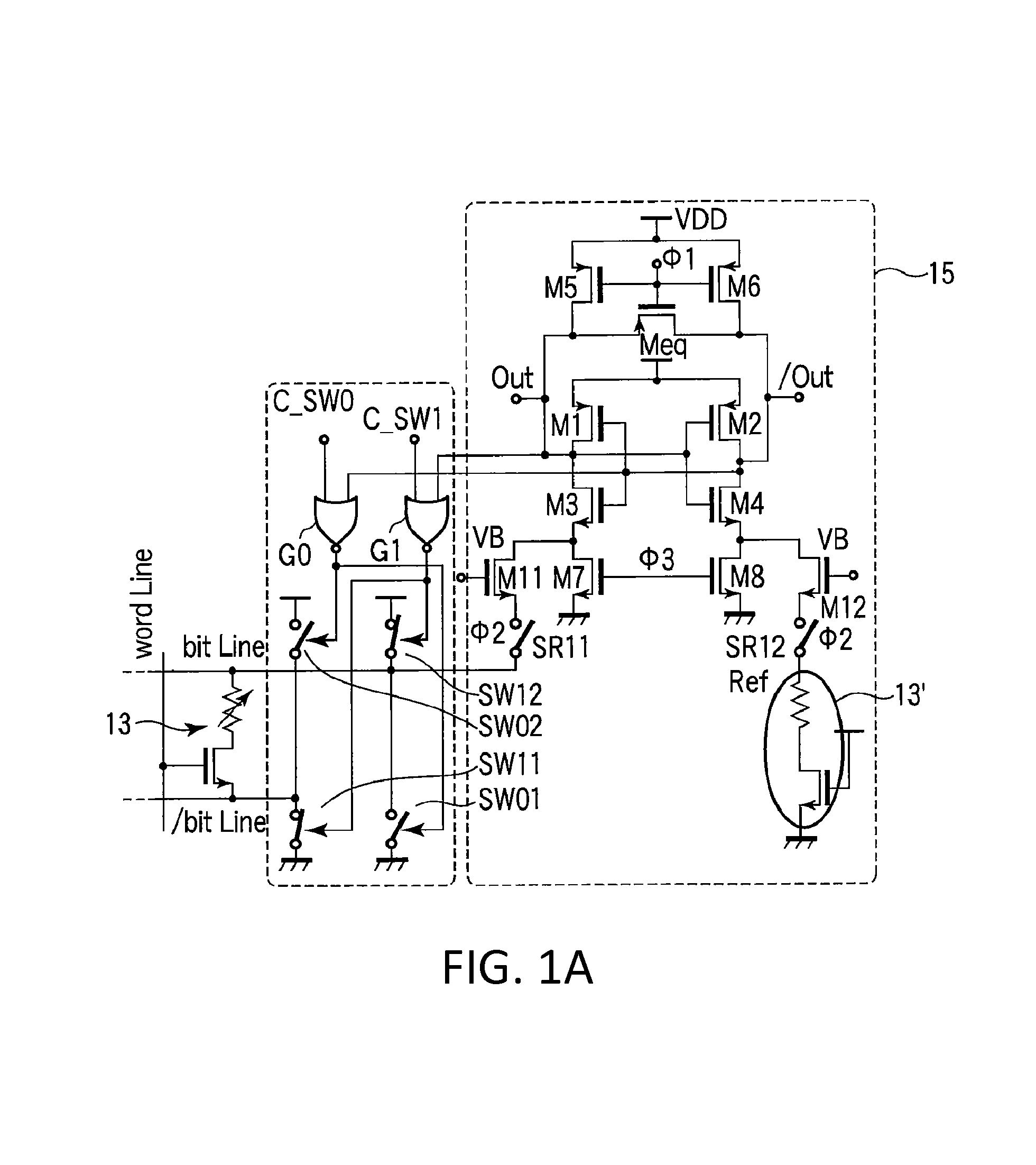
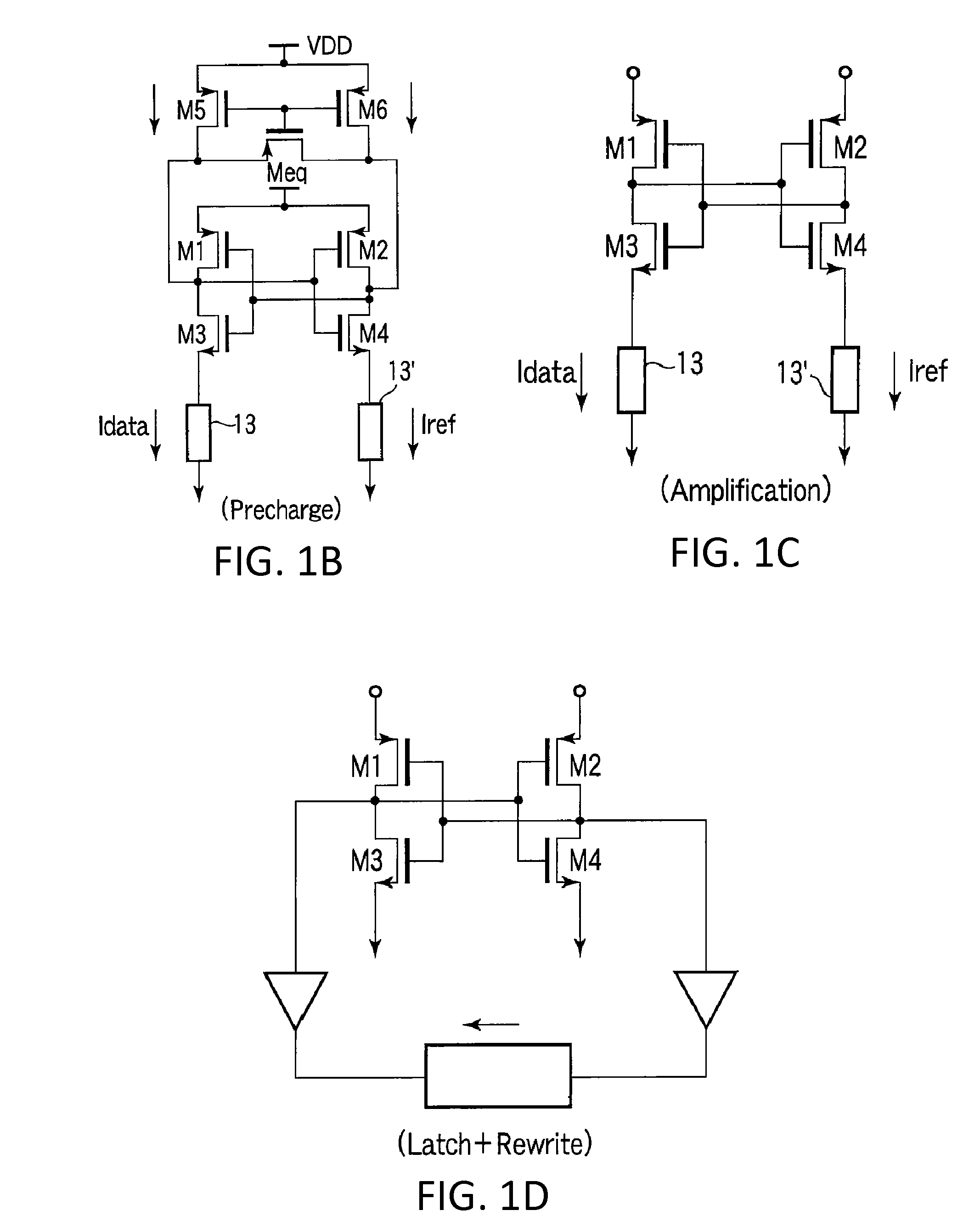
Embodiment Construction

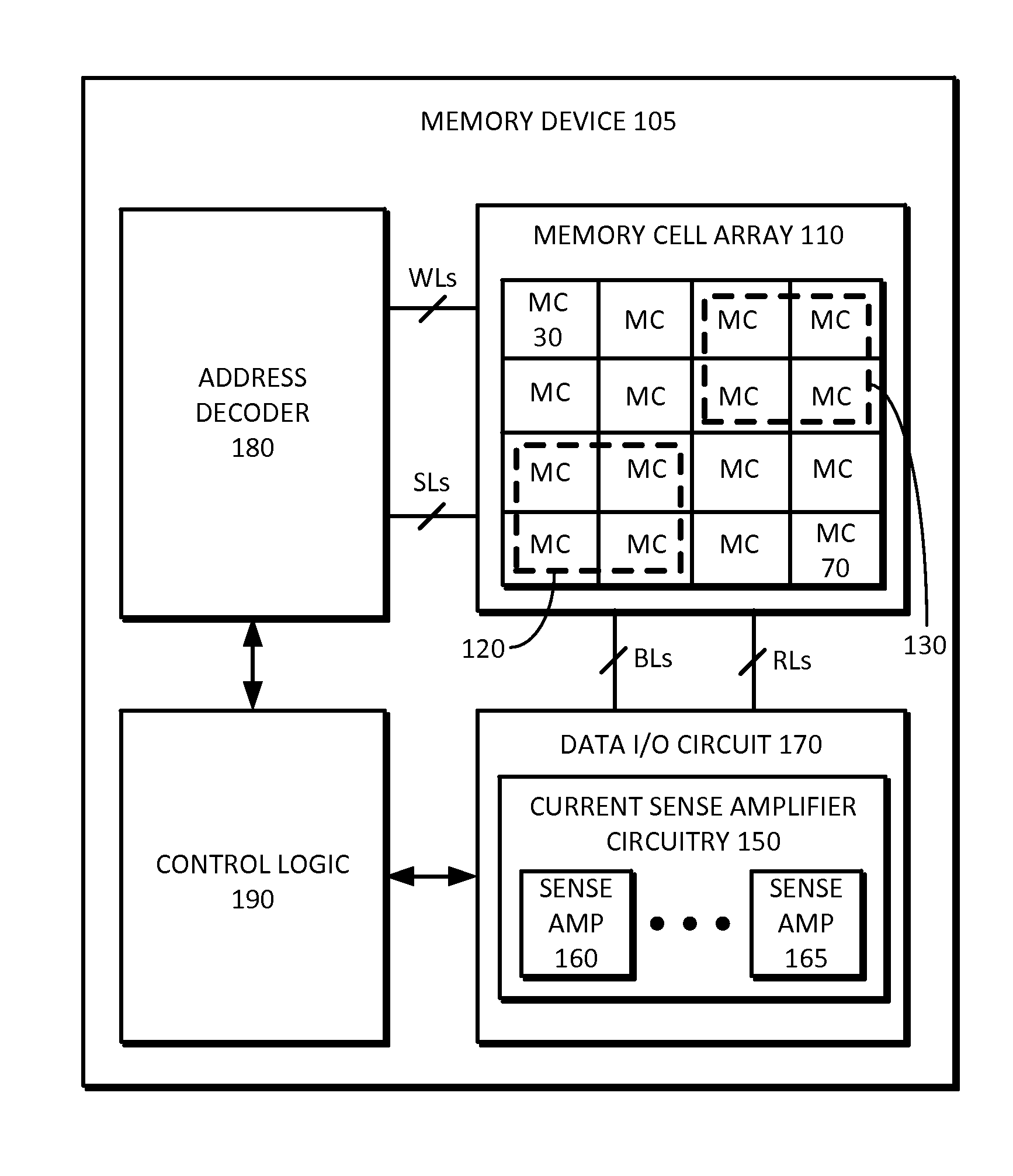
[0041]Reference will now be made in detail to embodiments of the invention, examples of which are illustrated in the accompanying drawings. In the following detailed description, numerous specific details are set forth to enable a thorough understanding of the present invention. It should be understood, however, that persons having ordinary skill in the art may practice the present invention without these specific details. In other instances, well-known methods, procedures, components, circuits, and networks have not been described in detail so as not to unnecessarily obscure aspects of the embodiments.

[0042]It will be understood that, although the terms first, second, etc. may be used herein to describe various elements, these elements should not be limited by these terms. These terms are only used to distinguish one element from another. For example, a first circuit could be termed a second circuit, and, similarly, a second circuit could be termed a first circuit, without departin...


PUM


Abstract

Example embodiments include a resistive type memory current sense amplifier circuit including differential output terminals, first and second input terminals, pre-charge transistors, and current modulating transistors coupled directly to the pre-charge transistors. The pre-charge configuration provides high peak currents to charge the bit line and reference line during a “ready” or “pre-charge” stage of operation of the current sense amplifier circuit. The current modulating transistors are configured to operate in a saturation region mode during at least a “set” or “amplification” stage. The current modulating transistors continuously average a bit line current and a reference line current during the “set” or “amplification” stage, thereby improving noise immunity of the circuit. During a “go” or “latch” stage of operation, a logical value “0” or “1” is latched at the differential output terminals based on positive feedback of a latch circuit.

Description

BACKGROUND[0001]The present inventive concepts relate to sense amplifiers for resistive type memory circuits, and more particularly to current sense amplifiers.[0002]Resistive type memories encompass a new generation of non-volatile memory and are expected to become more prevalent in the marketplace. Resistive type memories can include, for example, spin transfer torque (STT) magnetoresistive random-access memory (MRAM), MRAM (of the non-STT variety), memristor RAM, ReRAM, CBRAM, and the like.[0003]FIG. 1A is a circuit diagram of a sense amplifier according to the prior art. Referring to FIG. 1A, a latch circuit is configured by MOS transistors M1, M2, M3, and M4. MOS transistors M5 and M6 correspond to the read current source IR1 and the reference current source IR2, respectively. A sense amplifier is configured by MOS transistors M7 and M8. An operation of the read circuit 15 includes (a) a pre-charge mode, (b) an amplification mode, and (c) a latch+rewrite mode. The modes are des...

Claims


Application Information

Patent Timeline
Patent Type & Authority Applications(United States)
IPC IPC(8): G11C7/06G11C7/12G11C11/00
CPCG11C7/062G11C7/12G11C11/1653G11C11/1673G11C11/1675G11C13/0002G11C13/0007G11C13/0011G11C13/004G11C2013/0042G11C2207/063G11C7/06G11C13/00
Inventor YOUN, YONGSIKONG, ADRIAN E.CHA, SOOHOKIM, CHAN-KYUNG
Owner SAMSUNG ELECTRONICS CO LTD
Why Eureka
Try Eureka