Method of making dielectric capacitors with increased dielectric breakdown strength

a dielectric capacitor and breakdown strength technology, applied in the field of ceramic film capacitors, can solve the problems of affecting the manufacture of capacitors, containing, material and manufacturing limitations, and normal irregularities in the raw material or fabrication process that produce minor flaws or weaknesses within the capacitor structure, so as to reduce the catastrophic failure of the dielectric, block or slow down the growth of structural defects, and minimize the effect of physical variations

Active Publication Date: 2013-12-19
UCHICAGO ARGONNE LLC
View PDF21 Cites 19 Cited by
  • Summary
  • Abstract
  • Description
  • Claims
  • Application Information

AI Technical Summary

Benefits of technology

[0013]Another object of the present invention is to minimize the effect of physical variations within the dielectric. A feature of the invention is the formation of a better conductive zone to redistribute the charge over a larger area. An advantage of the invention is to provide an embedded barrier to block or slow down the growth of structural defects which act as a conduit/route for charge transfer between electrodes.
[0014]Another object of the present invention is to reduce catastrophic failure of the dielectric so as to reduce electrical damage to the host system. A feature of the invention is to provide a physical barrier within the dielectric material to slow down or block the propagation of a physical breaking in the dielectric. An advantage of the invention is the formation of a structure embedded within the dielectric to alleviate rapid occurring of dielectric breakdown.
[0015]In brief, the invention provides a process for forming a capacitor and a capacitor formed from dielectric material between two conductors with a conductive oxide layer embedded within dielectric at distance from either electrode. This invention comprises a method for fabrication of dielectric capacitors with increased dielectric breakdown strength, and more specifically, a method to enhance breakdown strength of a dielectric material through modification of material architecture. The dielectric material can be ceramic films on metal foils (film-on-foils) that can be stacked or embedded for producing high-performance practical capacitor devices.
[0016]In brief, in the present invention, the inventors disclose a process for making ceramic dielectric film capacitors with increased dielectric breakdown strength by embedding a thin conductive oxide ceramic layer within the matrix of ceramic dielectric materials and the resulting capacitor formed by the method.
[0017]The invention is directed a process of making ceramic film capacitors with increased dielectric breakdown strength, comprising: providing a bottom electrode; depositing a first dielectric layer on the bottom electrode; depositing a first conductive oxide on the first dielectric; depositing a second dielectric layer on the conductive oxide and depositing a top electrode, to form a laminated capacitor. In an embodiment of the invention the process further comprising attaching a first termination lead to the bottom electrode and attaching a second termination lead to the top electrode. The termination lead provides connection between electrode internal to the capacitor and other circuits.
[0018]In another embodiment of the invention the dielectric is selected from the group consisting of lead zirconate titanate [Pb(Zr,Ti)O3, PZT], lead lanthanum zirconate titanate [(Pb,La)(Zr,Ti)O3, PLZT], lead magnesium niobate [Pb(Mg1/3Nb2/3)O3, PMN], barium titanate [(BaTiO3), BT], strontium titanate [SrTiO3, ST], barium strontium titanate [(Ba,Sr)TiO3, BST],

Problems solved by technology

Fabrication of capacitors, containing at least two electrical conductors separated by a dielectric, is affected by material and manufacturing limitations.
Normal irregularities in the raw material or fabrication processes produce minor flaws or weaknesses within the capacitor structure.
Likewise, slight variations in the composition of the dielectric may result in differences in the localized physical and electrical properties within the dielectric.
Further, fabrication processes for formation of the dielectric layer on the conductor may produce voids, inclusions or micro cracks, which again may result in differences in the localized composition and properties within the dielectric.
When exposed to electric fields near the operating limits of the device these irregularities may concentrate the electric field over time to result in a breakdown of the device.
The dielectric breaks down when the current rises sharply at a critical electric field; permanent damage is often found along fine tubular channels or cracks, the major portion of the sample being left intac

Method used


Image

  • Method of making dielectric capacitors with increased dielectric breakdown strength
  • Method of making dielectric capacitors with increased dielectric breakdown strength
  • Method of making dielectric capacitors with increased dielectric breakdown strength

Examples


Embodiment Construction

[0031]The foregoing summary, as well as the following detailed description of certain embodiments of the present invention, will be better understood when read in conjunction with the appended drawings.

[0032]As used herein, an element or step recited in the singular and preceded with the word “a” or “an” should be understood as not excluding plural said elements or steps, unless such exclusion is explicitly stated. Furthermore, references to “one embodiment” of the present invention are not intended to be interpreted as excluding the existence of additional embodiments that also incorporate the recited features. Moreover, unless explicitly stated to the contrary, embodiments “comprising” or “having” an element or a plurality of elements having a particular property may include additional such elements not having that property.

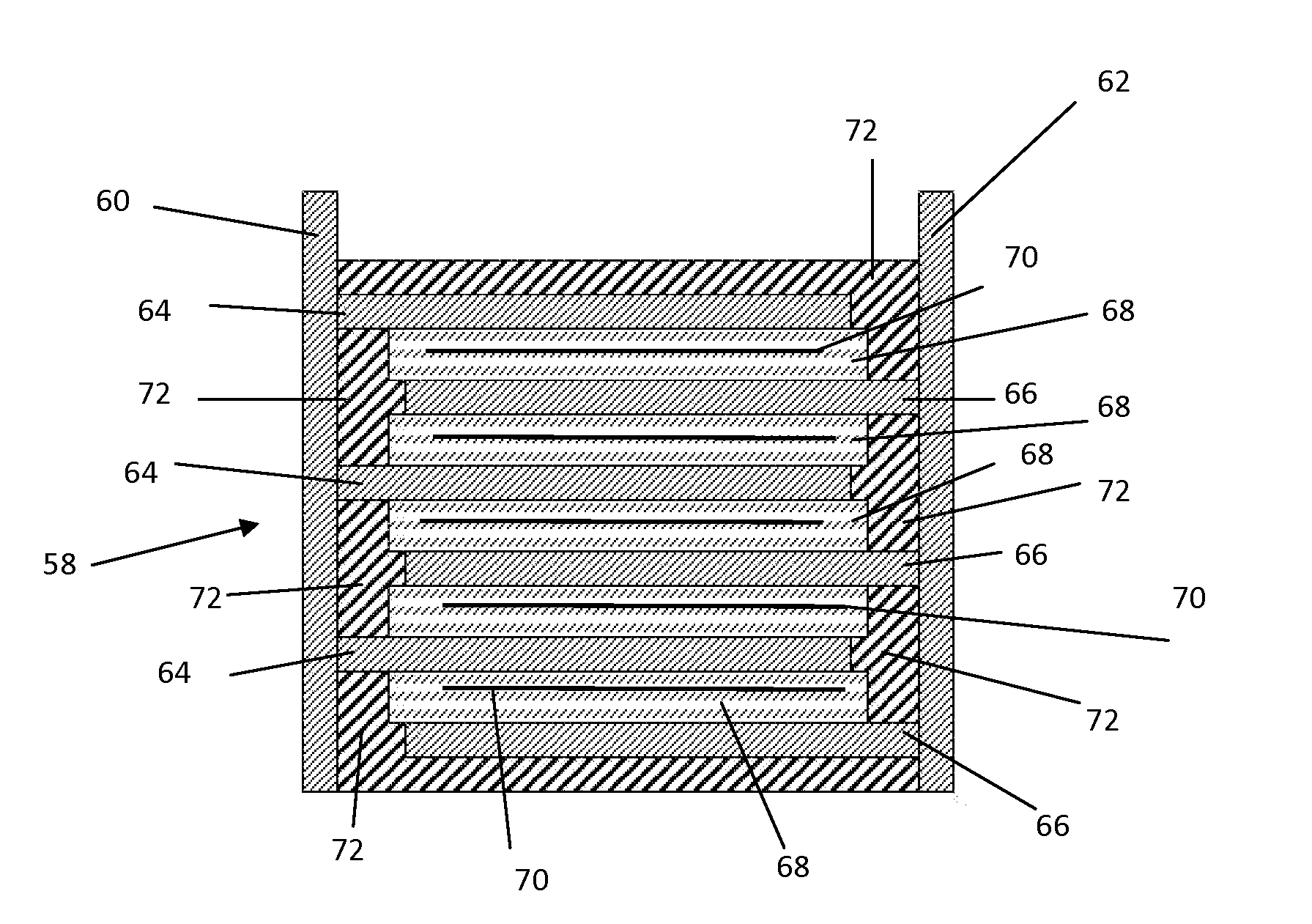
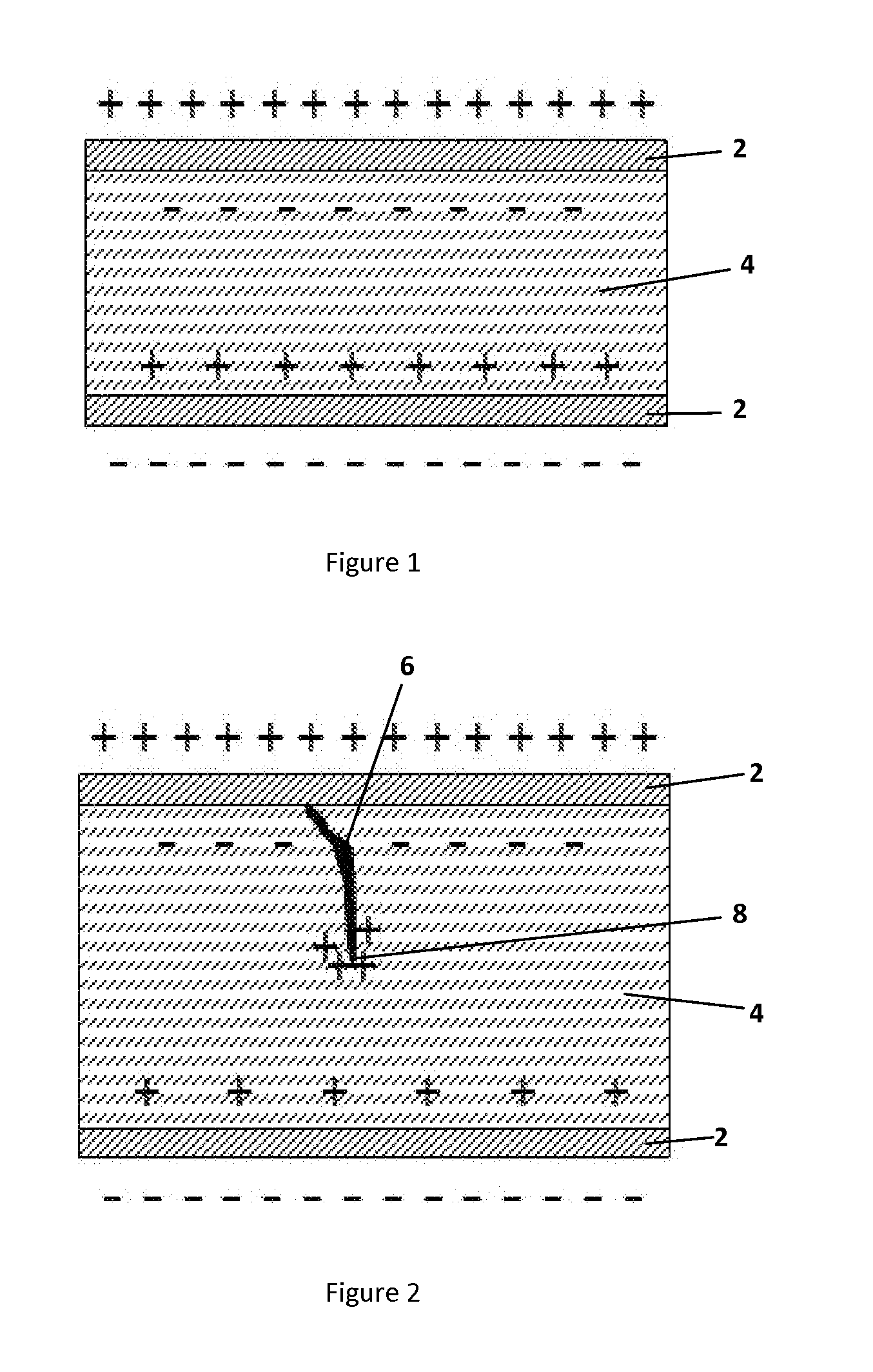
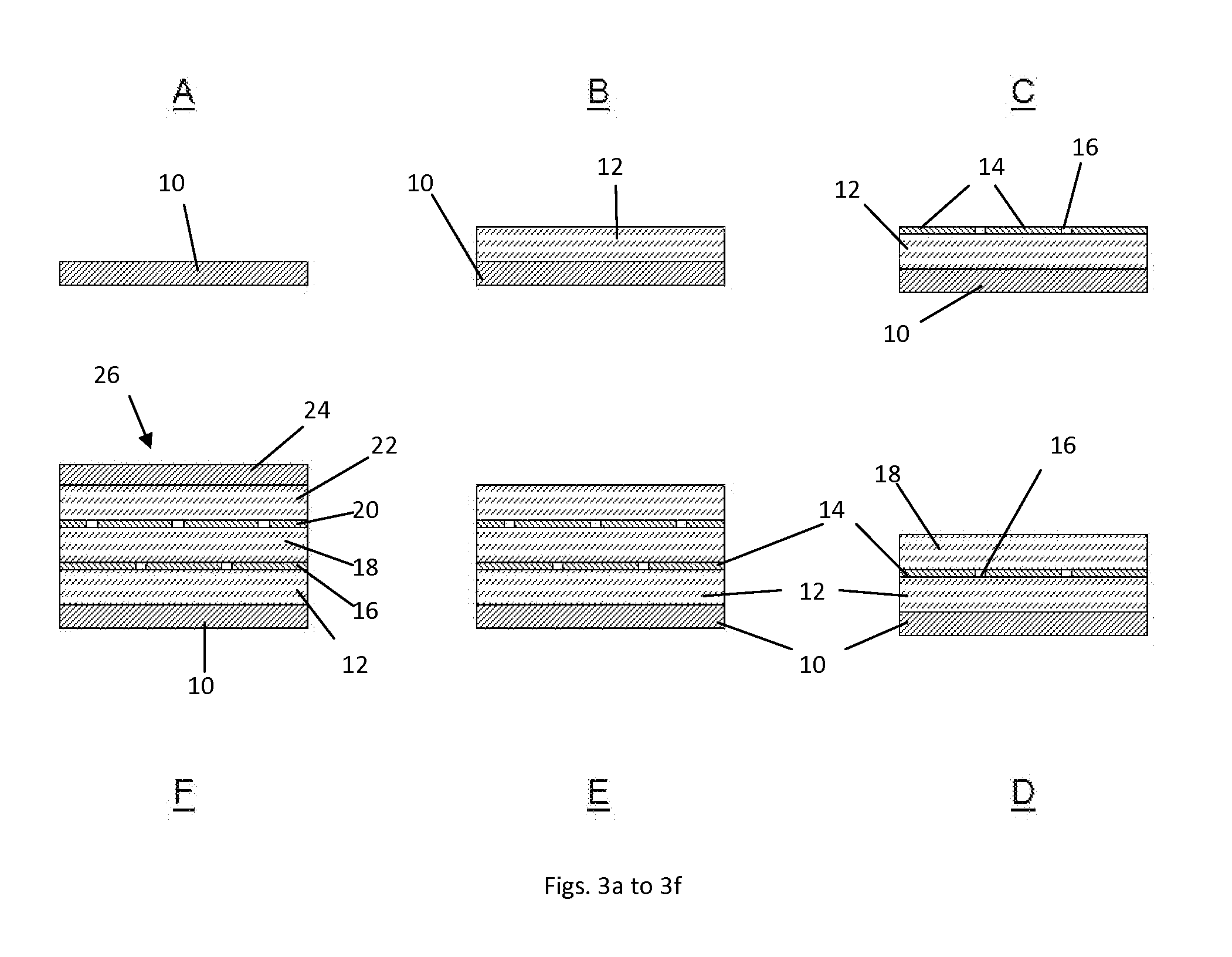
[0033]The inventors have developed a process of fabricating high capacitance density dielectric film capacitors, and in particular ceramic film capacitors. Whe...


PUM

PropertyMeasurementUnit
Thicknessaaaaaaaaaa
Thicknessaaaaaaaaaa
Thicknessaaaaaaaaaa

Abstract

The invention is directed to a process for making a dielectric ceramic film capacitor and the ceramic dielectric laminated capacitor formed therefrom, the dielectric ceramic film capacitors having increased dielectric breakdown strength. The invention increases breakdown strength by embedding a conductive oxide layer between electrode layers within the dielectric layer of the capacitors. The conductive oxide layer redistributes and dissipates charge, thus mitigating charge concentration and micro fractures formed within the dielectric by electric fields.

Description

CONTRACTUAL ORIGIN OF THE INVENTION[0001]The U.S. Government has rights in this invention pursuant to Contract No. DE-AC02-06CH11357 between the U.S. Department of Energy and UChicago Argonne, LLC.FIELD OF THE INVENTION[0002]The present invention relates to formation of high performance ceramic dielectric films. This invention relates to ceramic film capacitors, and more particularly, relates to compact and high energy density ceramic film capacitors, their associated structure and method of fabrication.BACKGROUND OF THE INVENTION[0003]The development of power electronic devices with improved performance, increased reliability, compacted size, and reduced weight requires the passive components, such as resistors, capacitors, inductors, and transformers, to be stacked or embedded within a printed wire board (PWB). This technology could free up surface space, increase device reliability, and minimize electromagnetic interference and inductance loss. The capacitance density of a dielec...

Claims


Application Information

Patent Timeline
IPC IPC(8): H01G4/12H01G4/10H01G4/008H01G4/00
CPCH01G4/008H01G4/10H01G4/12H01G4/1209H01G4/30Y10T29/435
Inventor MA, BEIHAIBALACHANDRAN, UTHAMALINGAMLIU, SHANSHAN
Owner UCHICAGO ARGONNE LLC
Why Eureka
Try Eureka