One of the current challenges for
mass-scale world-wide deployment of photovoltaic (PV) systems is the reduction of the levelized cost of
electricity (LCOE) for the electricity generated from PV systems below that of conventional fossil fuels, without reliance on subsidies and regulatory support.
However, currently direct
band gap materials, such as mono-crystalline direct gap band materials (for example group III-V materials) and particularly GaAs), have not been fully realized in
mass-scale and broad commercial implementations (including for residential and commercial rooftops).
Thus, it may be considered highly inefficient to use an expensive material such as a GaAs
wafer for mechanical support.
These methods may reuse the expensive GaAs
wafer as a reusable template, hence, amortizing the cost of the starting GaAs wafer over multiple reuse cycles.
However, since GaAs wafers are very expensive (and also far more limited in size compared to
silicon wafers), in most instances the GaAs wafer used as a reusable template has to be reused at least hundreds of times with extremely high (e.g., 99.9% or more) yield without breakage in order to reduce the resulting
solar cell costs significantly and make them competitive compared to the mainstream traditional
silicon solar cell technologies (in terms of
cell cost per
watt).
This poses significant technological and manufacturing challenges for commercial viability of GaAs wafer as a reusable template for cost-effective
photovoltaics.
Furthermore and importantly, this method is practically limited to the production of a smaller sized GaAs solar
cell size (for instance, up to 100 mm×100 mm or at most 125 mm×125 mm) because of prohibitively expensive cost of GaAs wafers as well as the technological difficulties and economic challenges of producing and
processing large area GaAs wafers (for instance, 200-mm in
diameter or 156 mm×156 mm
cell dimensions) on which the GaAs solar cell is formed and processed.
While high efficiency, single-junction and multi-junction cells have been made and demonstrated using III-V materials such as GaAs in the past, these structures and manufacturing processes have been plagued and limited by the very high cost of the starting wafer which has prevented their widespread penetration into the mainstream terrestrial PV market (excluding the CPV market segment for certain ground-
mount utility applications in high DNI solar
radiation regions).
It is well known that the cost of GaAs wafers is significantly higher than that of
silicon wafers, while the largest economically viable GaAs wafers are substantially smaller than the corresponding silicon wafers.
Historically, a GaAs
cell fabrication process may start with a
semiconductor substrate such as
Germanium (Ge) or GaAs and build GaAs based solar cells on top of these very expensive substrates (it is be noted Ge wafers are also very expensive as compared to Si wafers).
However, there are several problems with this conventional III-V compound
semiconductor material based solar cell and fabrication process, particularly relating to cost and
scalability:The starting substrates (such as GaAs or Ge wafers) are relatively expensive and substantially more expensive as compared to Si.The starting substrates / wafers are typically smaller, in the range of approximately 75 mm up up to 150 mm in
diameter, and substantially smaller as compared to prevalent Si substrates / wafers which are routinely 200 mm to 300 mm in
diameter (prototypes of 450 mm diameter
CZ silicon wafers have been demonstrated as well) and 156 mm×156 mm squares (or 210 mm×210 mm squares) for solar cells.
In order to make them relatively cost-effective for certain ground-
mount utility applications, small area compound
semiconductor solar cells are almost exclusively used in very high-concentration PV (CPV) applications, often requiring expensive and large concentrators and multi-axis trackers (and in some cases liquid cooling of the solar cells).Conventional III-V semiconductor based solar cells often use and rely on unconventional and expensive cell packaging schemes which do not have the economies of scale as
silicon based PV modules (particularly for applications without concentrators).Despite a higher cell efficiency, of the primary issues with compound semiconductor solar cells and modules relate to the very high cost of the starting material (GaAs or Ge wafers), manufacturing methods (such as relatively low-
throughput MOCVD systems), and additional cost of Balance of Systems (BOS) of compound semiconductor CPV systems, including concentrators and trackers (and cooling systems).
These issues make the overall
system level cost ($ /
Watt) metric relatively high.
Although, this may represent an economic (cost reduction) improvement to the previous III-V semiconductor solar cell manufacturing schemes, this approach may also suffer from serious manufacturing challenges (such as the limited reuse number of the extremely brittle, fragile, and expensive GaAs wafers) relating to manufacturing cost and
scalability for widespread terrestrial mass deployment and adoption, particularly in the market segments where
crystalline silicon PV is dominant (for instance the residential and commercial rooftop markets in particular, as well as even the ground
mount utility scale PV installations).
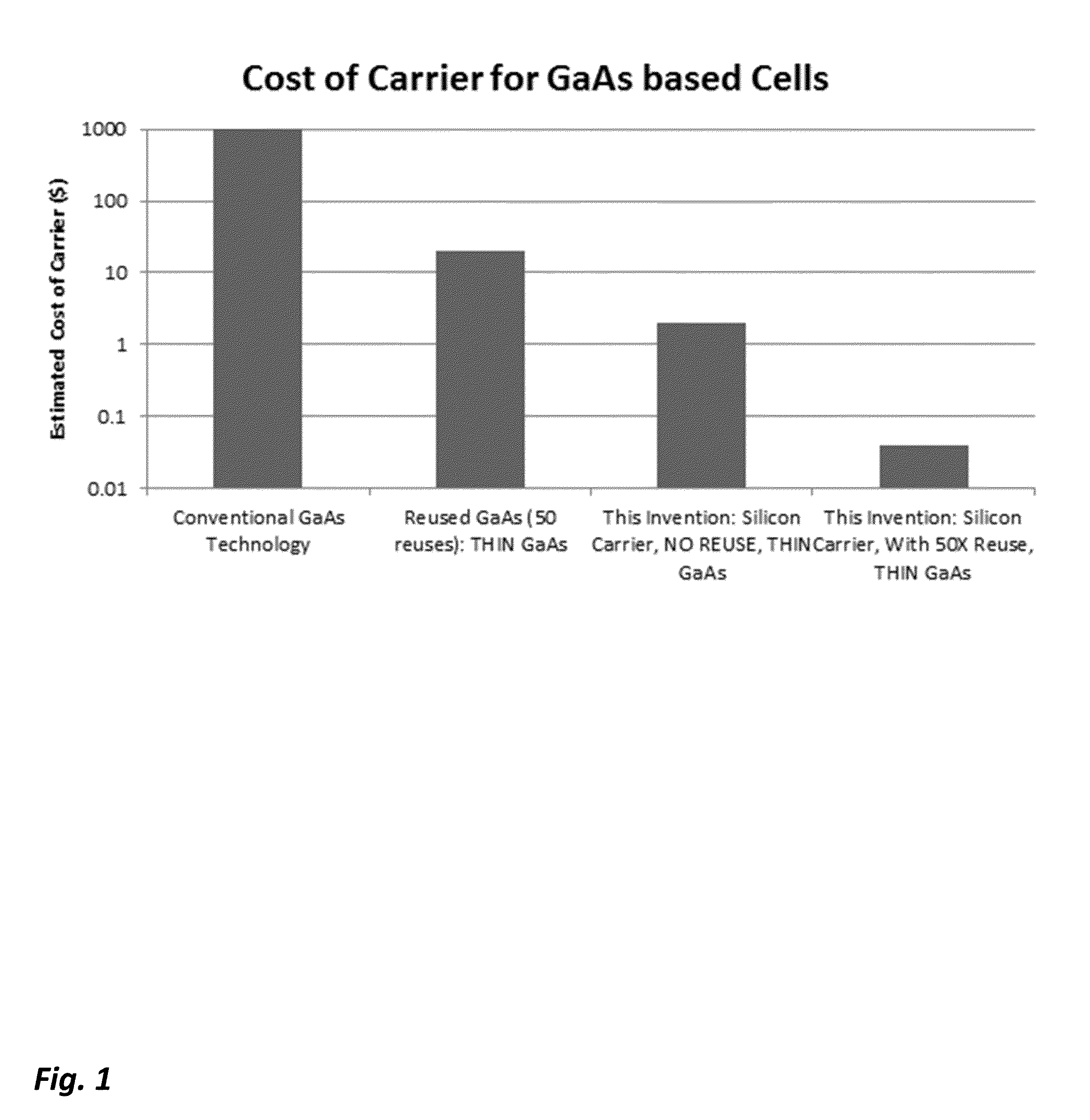
For example:Because of the high cost of the GaAs (and Ge) wafers, the GaAs (or Ge) wafer will have to be reused at least several hundred times without any breakage and without any degradation of the surface quality in order to ensure that the amortized starting wafer cost is not a significant contributor to the overall cost of the resulting III-V solar cells and modules.Since GaAs is intrinsically a brittle and fragile semiconductor material, reuse yield of this material for several hundred times without breakage is extremely challenging and difficult.
Hence, there is a large reuse performance gap between what has been shown or can be demonstrated (10's of cycles at maximum) and what's required (at least 100's of cycles) to achieve the desired manufacturing cost targets.The size of the solar cell is limited by the size of the widely available starting GaAs wafers, resulting in low
power output per cell despite relatively
high cell efficiency.
Current available GaAs wafer size is in the range of up to about 150 mm diameter (compared to much larger size of
Silicon substrates: 200 mm to 300 mm in diameter), making the largest practical solar cell sizes about 100 mm×100 mm full square or about 125 mm×125 mm pseudo square.Handling of the thin (typically <5 microns) GaAs solar cell absorber stack layer after it is detached from the carrier GaAs wafer can be quite challenging and costly depending on the scheme deployed.
Furthermore, GaAs is a very brittle and fragile material and problems relating to GaAs substrate
processing yield and
structural integrity are substantially compounded as the substrate size (area) increases.
For example, cost effective high volume MOCVD reactors are not yet commercially available for
mass scale solar cell manufacturing.
The commercially available MOCVD and MBE tools have relatively small batch sizes and result in very low production throughputs, typically on the order of a few to 10's of wafers per hour.

