Pulse output circuit and semiconductor device

Active Publication Date: 2014-01-02
SEMICON ENERGY LAB CO LTD
View PDF4 Cites 16 Cited by
  • Summary
  • Abstract
  • Description
  • Claims
  • Application Information

AI Technical Summary

Benefits of technology

The present invention provides a semiconductor device that can prevent the threshold voltage of a transistor from shifting due to deterioration. By decreasing the amplitude of the control signal that regulates the potential applied to a bus line, the device prevents damage to the transistor while still maintaining the desired output signal amplitude. This results in a highly reliable semiconductor device that can maintain optimal performance over time.

Problems solved by technology

However, when the amplitude of the control signal is decreased, the amplitude of a potential applied from the other of the source and the drain of the transistor to the bus line is also decreased, which is unfavorable.

Method used


Image

  • Pulse output circuit and semiconductor device
  • Pulse output circuit and semiconductor device
  • Pulse output circuit and semiconductor device

Examples


embodiment 1

[0044]In this embodiment, examples of a pulse output circuit included in a driver circuit according to one embodiment of the present invention are described.

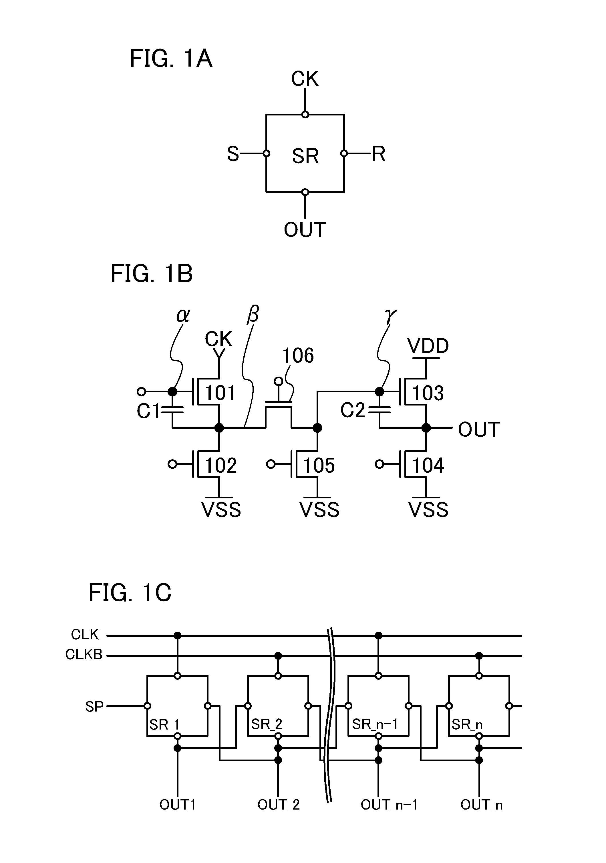
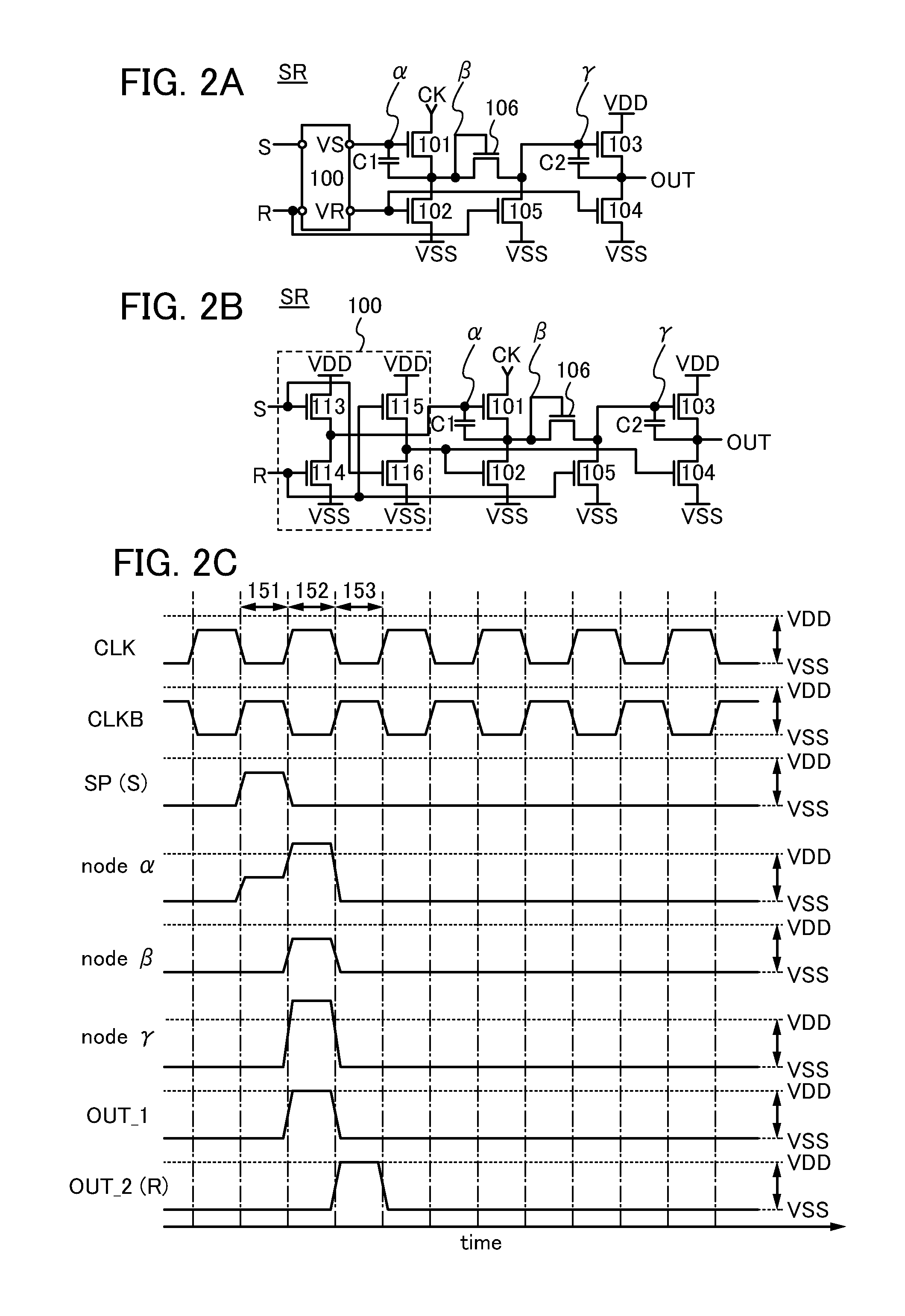
[0045]FIGS. 1A to 1C illustrate a structure example of a pulse output circuit in this embodiment. A pulse output circuit SR in FIGS. 1A to 1C has a function of outputting a pulse signal through an output end (OUT) in response to a set signal (S), a reset signal (R), and a clock signal (CK) that are input, as illustrated in FIG. 1A. Note that a plurality of clock signals may be input to the pulse output circuit SR.

[0046]The pulse output circuit SR in FIG. 1A includes transistors 101 to 106, as illustrated in FIG. 1B. The transistors 101 to 106 have the same conductivity type.

[0047]For example, the plurality of pulse output circuits SR in FIG. 1A (pulse output circuits SR_1 to SR_n (n is a natural number of 2 or more)) are used to constitute a shift register, as illustrated in FIG. 1C. In FIG. 1C, n is 4 or more. At this time, a s...

embodiment 2

[0145]In a semiconductor device according to one embodiment of the present invention, a transistor may include a channel formation region in a semiconductor film of amorphous, microcrystalline, polycrystalline, or single crystal silicon, germanium, or the like. Alternatively, the transistor may include a channel formation region in a semiconductor film whose bandgap is wider than that of silicon and whose intrinsic carrier density is lower than that of silicon. Any of the following can be used as silicon: amorphous silicon formed by sputtering or vapor deposition such as plasma-enhanced CVD; polycrystalline silicon obtained in such a manner that amorphous silicon is crystallized by laser annealing or the like; single crystal silicon obtained in such a manner that a surface portion of a single crystal silicon wafer is separated by implantation of hydrogen ions or the like into the silicon wafer; and the like.

[0146]A highly-purified oxide semiconductor (a purified oxide semiconductor)...

embodiment 3

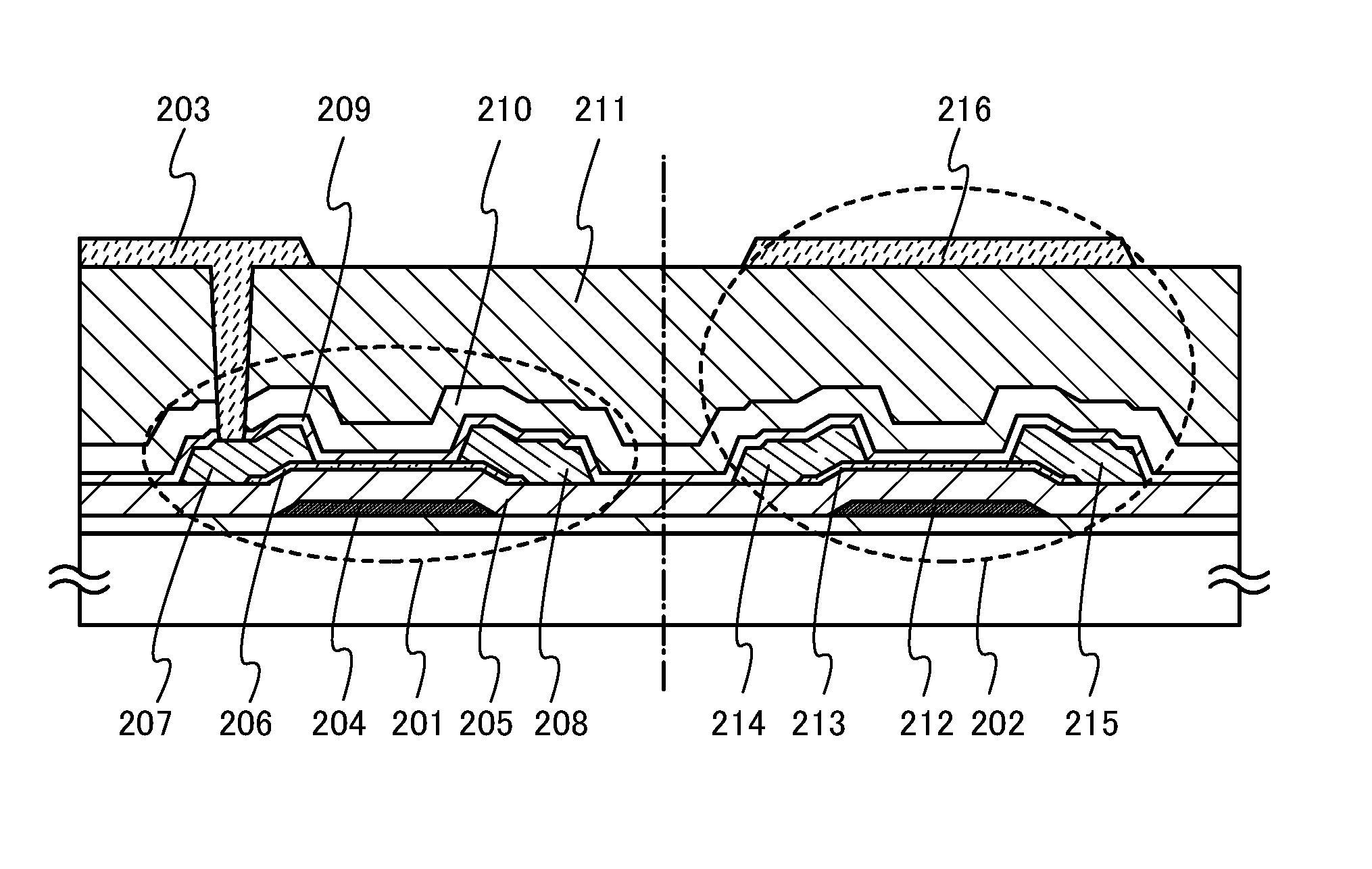
[0282]Next, an appearance of a liquid crystal display device according to one embodiment of the present invention is described with reference to FIGS. 13A to 13C. FIG. 13A is a top view of a liquid crystal display device where a substrate 4001 and a substrate 4006 are bonded to each other with a sealant 4005. FIG. 13B corresponds to a cross-sectional view taken along broken line A1-A2 in FIG. 13A. FIG. 13C corresponds to a cross-sectional view taken along broken line B1-B2 in FIG. 13A. Note that FIGS. 13A to 13C illustrate a fringe field switching (FFS)-mode liquid crystal display device.

[0283]The sealant 4005 is provided to surround a pixel portion 4002 and a pair of scan line driver circuits 4004 provided over the substrate 4001. The substrate 4006 is provided over the pixel portion 4002 and the scan line driver circuit 4004. Thus, the pixel portion 4002 and the scan line driver circuit 4004 are sealed by the substrate 4001, the sealant 4005, and the substrate 4006.

[0284]A signal ...


PUM


Abstract

A highly reliable semiconductor device in which a shift in threshold voltage of a transistor due to deterioration can be inhibited is provided. A pulse output circuit includes a first transistor, a second transistor, a third transistor, a fourth transistor, a fifth transistor, and a sixth transistor. A clock signal is supplied to a drain of the first transistor. A first power supply potential is applied to a source of the second transistor, and a drain of the second transistor is connected to the drain of the first transistor. A second power supply potential is applied to a drain of the third transistor. The first power supply potential is applied to a source of the fourth transistor, and a drain of the fourth transistor is connected to the drain of the third transistor. The first power supply potential is applied to a source of the fifth transistor, and a drain of the fifth transistor is connected to a gate of the third transistor. One of a source and a drain of the sixth transistor is connected to the drain of the first transistor, and the other of the source and the drain of the sixth transistor is connected to the gate of the third transistor. The first transistor and the third transistor include back gates connected to each other. The first to sixth transistors have the same conductivity type.

Description

BACKGROUND OF THE INVENTION[0001]1. Field of the Invention[0002]The present invention relates to pulse output circuits that include transistors having the same conductivity type, and semiconductor devices such as semiconductor display devices that include the pulse output circuits.[0003]2. Description of the Related Art[0004]Semiconductor display devices such as liquid crystal display devices and EL display devices preferably include transistors having the same conductivity type rather than CMOS transistors in order to reduce the cost of backplanes (circuit boards). Patent Documents 1 and 2 disclose techniques for forming a variety of circuits such as inverters and shift registers that are used in driver circuits of semiconductor display devices and are constituted of transistors having the same conductivity type.[0005]In particular, for a semiconductor display device including oxide semiconductor transistors, a glass substrate of the fifth generation (1200 mm wide×1300 mm long) or ...

Claims


Application Information

Patent Timeline
IPC IPC(8): H03K3/01
CPCH03K3/01G11C19/28G09G3/3688
Inventor TANADA, YOSHIFUMISATO, MANABUMIYAKE, HIROYUKISASAKI, TOSHINARIOKAZAKI, KENICHIKOEZUKA, JUNICHIYAMAZAKI, SHUNPEI
Owner SEMICON ENERGY LAB CO LTD
Why Eureka
Try Eureka