Three-dimensional thermoelectric energy harvester and fabrication method thereof

Active Publication Date: 2014-01-30
SHANGHAI INST OF MICROSYSTEM & INFORMATION TECH CHINESE ACAD OF SCI
View PDF12 Cites 6 Cited by
  • Summary
  • Abstract
  • Description
  • Claims
  • Application Information

AI Technical Summary

Benefits of technology

The present invention provides a three-dimensional thermoelectric energy harvester and a fabrication method thereof. The method involves etching a silicon substrate to form grooves and silicon columns, and then filling the grooves with thermoelectric material to form thermoelectric columns. A metal wiring is fabricated to connect the thermoelectric columns and a neighboring silicon column in a thermocouple pair. The substrate is then thinned and a lower supporting substrate is bonded to the upper substrate. The use of vertical thermocouple pairs and bonding at the wafer level improves the mechanical stability and fabrication efficiency of the thermoelectric energy harvester.

Problems solved by technology

In environmental extremes or other occasions unreachable to human beings, or when a network node moves or changes, it is difficult or even impossible to replace a battery, making it crucial to effectively provide energy to a node of the Internet of Things.
Since the metal material such as Cu or Ni is a conductor structure having a small Seebeck coefficient, thermoelectric energy harvesting chips fabricated by using the metal material such as Cu or Ni as the thermoelectric material generally have low efficiency.
However, the BiTe-based material requires a high cost, and contains toxic substances, which limits the use of BiTe thermoelectric energy harvesting chips.
In addition, since the composition of a thermocouple requires two thermoelectric materials, the vertical-type thermoelectric energy harvester generally needs to be subjected to two electroplating or thin-film sputtering deposition processes in order to fabricate a thermocouple material, which further increases the cost of the thermoelectric energy harvesting chip.
Moreover, the fabrication efficiency of the vertical-type thermoelectric energy harvester is low, because the thermoelectric energy harvester is thermally and mechanically connected to the upper and lower substrates through chip-level bonding.

Method used


Image

  • Three-dimensional thermoelectric energy harvester and fabrication method thereof
  • Three-dimensional thermoelectric energy harvester and fabrication method thereof
  • Three-dimensional thermoelectric energy harvester and fabrication method thereof

Examples


embodiment 1

[0057]Referring to FIG. 2 to FIG. 11, the present invention provides a method for fabricating a three-dimensional thermoelectric energy harvester, which at least includes the following steps.

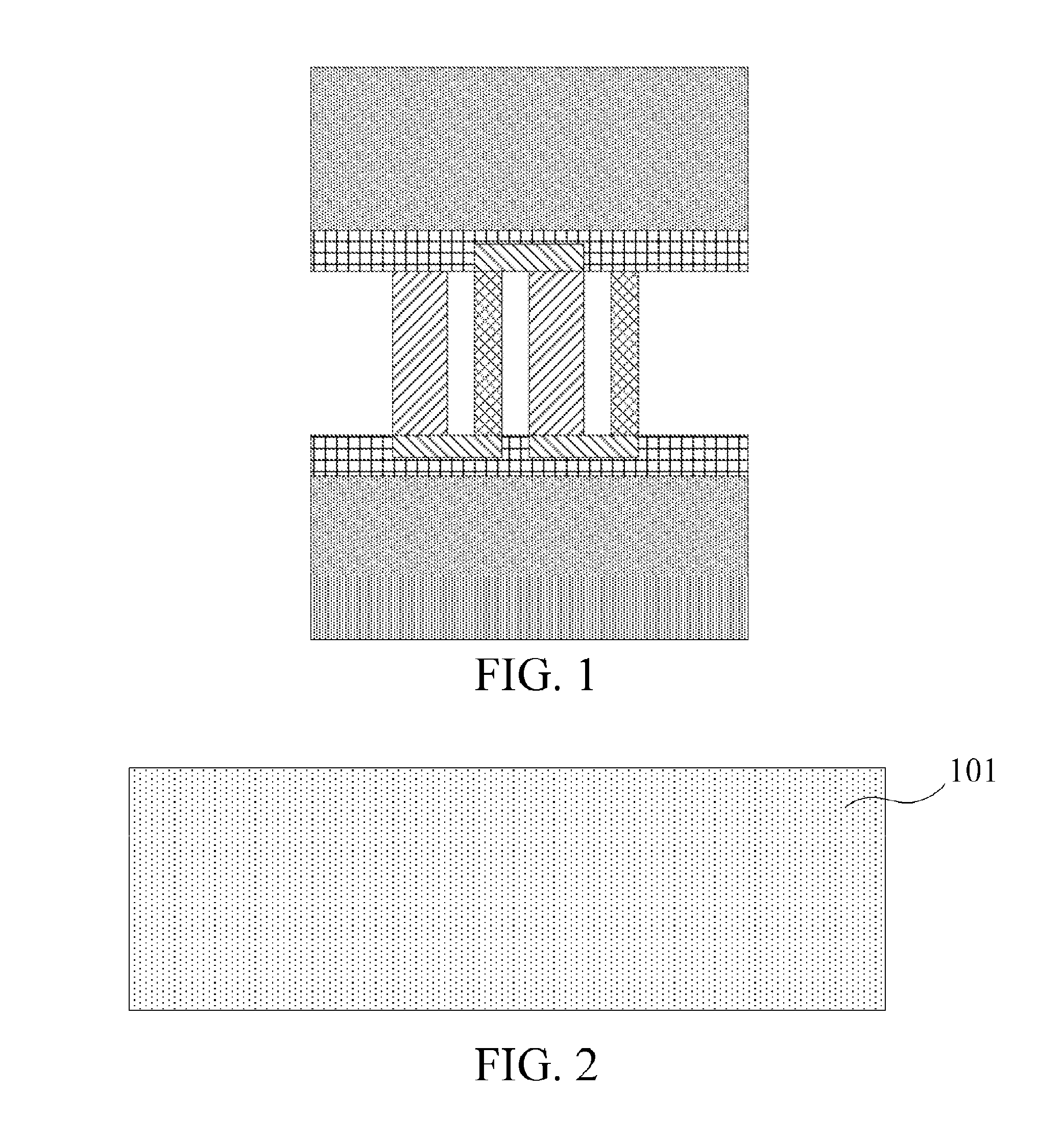
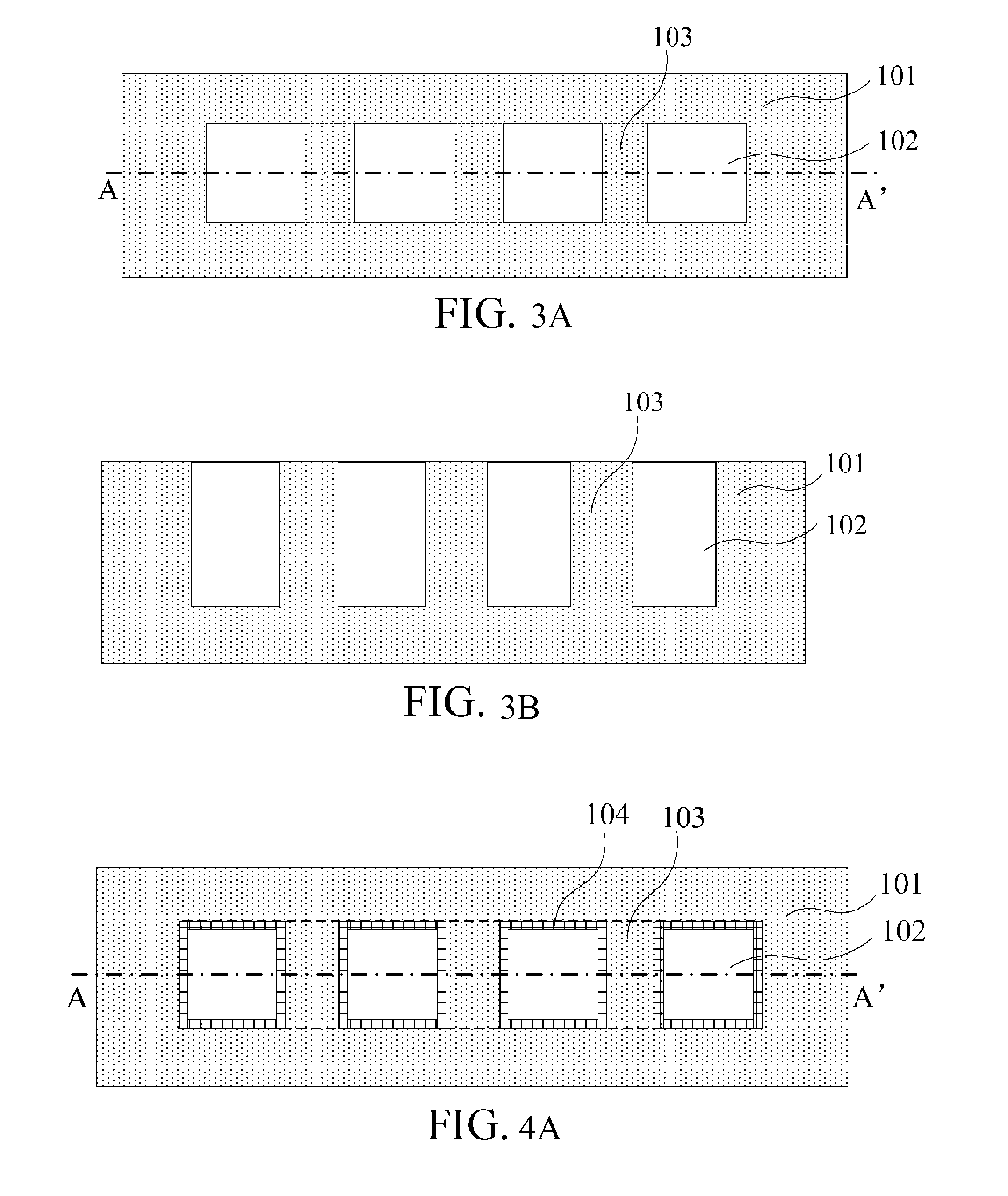
[0058]First, as shown in FIG. 2 to FIG. 3B, step 1) is performed, wherein a silicon substrate 101 is provided, and an upper surface of the silicon substrate 101 is etched to form a plurality of grooves 102, two neighboring of which are arranged at an interval, so that the grooves 102 and regions for preparing silicon columns 103 between the grooves 102 form a thermopile region. In this embodiment, the silicon substrate 101 is a low-resistivity silicon substrate 101, which has a high Seebeck coefficient and low resistivity, and therefore can ensure high thermoelectric efficiency when being fabricated into a thermoelectric column. To ensure a precise process, in this step, the low-resistivity silicon substrate 101 is polished first, and then a photolithographic pattern is fabricated on a surface o...

embodiment 2

[0065]Referring to FIG. 2 to FIG. 10B and FIG. 12, basic steps of the method for fabricating a three-dimensional thermoelectric energy harvester in this embodiment are as described in Embodiment 1. To further improve the mechanical stability and thermoelectric efficiency of a thermopile, the step 7) further includes a step of filling an electrical and thermal insulating material 109 in the annular groove 108.

embodiment 3

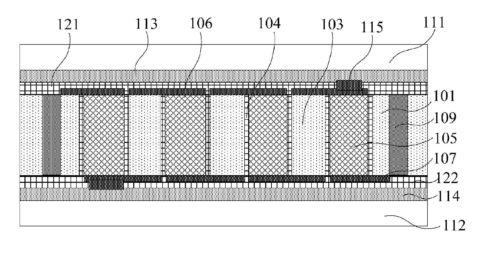
[0066]Referring to FIG. 2 to FIG. 10B, FIG. 13 and FIG. 14, basic steps of the method for fabricating a three-dimensional thermoelectric energy harvester in this embodiment are as described in Embodiment 1 or 2. To achieve monolithic integration of the three-dimensional thermoelectric energy harvester consistent with the present invention and a circuit so as to directly supply power to the circuit on-chip, the method for fabricating a three-dimensional thermoelectric energy harvester consistent with the present invention further includes a step of fabricating CMOS circuit structures 113 and 114 on the upper supporting substrate 111 and the lower supporting substrate 112, wherein the upper passivation layer 121 and the lower passivation layer 122 each are etched to form a contact hole 115, and then metal wires are fabricated through the contact holes 115 to respectively connect the CMOS circuits structures and the upper metal wiring and the lower metal wiring. Afterward, the upper pa...


PUM


Abstract

A three-dimensional thermoelectric energy harvester and a fabrication method thereof. Low-resistivity silicon is etched to form a plurality of grooves and silicon columns between the grooves, and an insulating layer is formed on a surface of the groove, and thermoelectric columns are fabricated by using a thin-film deposition technique, so that the thermoelectric column and a neighboring silicon column form a thermocouple pair; and then, a metal wiring is fabricated by processes such as etching and deposition, followed by thinning of the substrate and bonding of the supporting substrates, thereby completing fabrication of the three-dimensional thermoelectric energy harvester. Fabrication of the thermocouple pair structure by one thin-film deposition process simplifies the fabrication process. The thermocouple pair using silicon ensures a high Seebeck coefficient. The use of vertical thermocouple pairs having a column structure improves the mechanical stability of the thermoelectric energy harvester.

Description

BACKGROUND OF THE PRESENT INVENTION[0001]1. Field of Invention[0002]The present invention relates to the semiconductor field, and specifically to a three-dimensional thermoelectric energy harvester and a fabrication method thereof.[0003]2. Description of Related Art[0004]With the development of the Internet of Things, its applications in the industrial, commercial, medical, consumption and military fields are gradually expanded. Power source is always critical to prolonging the service life and reducing the cost of the Internet of Things. In environmental extremes or other occasions unreachable to human beings, or when a network node moves or changes, it is difficult or even impossible to replace a battery, making it crucial to effectively provide energy to a node of the Internet of Things. An effective solution is to harvest ambient energy through energy harvesting, store the energy and provide the energy to the node of the Internet of Things. Temperature difference is widely prese...

Claims


Application Information

Patent Timeline
IPC IPC(8): H01L35/32H01L35/34
CPCH01L35/34H01L35/32H10N19/00H10N10/01H10N10/17
Inventor XU, DEHUIXIONG, BINWANG, YUELIN
Owner SHANGHAI INST OF MICROSYSTEM & INFORMATION TECH CHINESE ACAD OF SCI
Why Eureka
Try Eureka