
Power light emitting diode and method with uniform current density operation

a power light emitting diode and current density technology, applied in the field of lighting techniques, can solve the problems of reducing active area utilization, practical limit on die size, and reducing the size of lateral chips, so as to achieve high current density, easy to form, and high yield

Active Publication Date: 2014-01-30
KORRUS INC
View PDF10 Cites 14 Cited by
  • Summary
  • Abstract
  • Description
  • Claims
  • Application Information

AI Technical Summary

Benefits of technology

This patent describes a new LED chip design and manufacturing process that can achieve higher yields and smaller feature sizes, compared to conventional techniques. The design reduces the amount of semiconductor material needed for the lighting product, which increases production efficiency and reduces costs. The use of a thin LED chip design also allows for efficient assembly of the optics and components used in the final product. The resulting LED device has no droop and operates at high current densities. The LED active region design is particularly beneficial for reducing droop, which enables higher current densities and efficient operation. Overall, this patent provides a more efficient and cost-effective solution for producing high-quality LED lighting.

Problems solved by technology

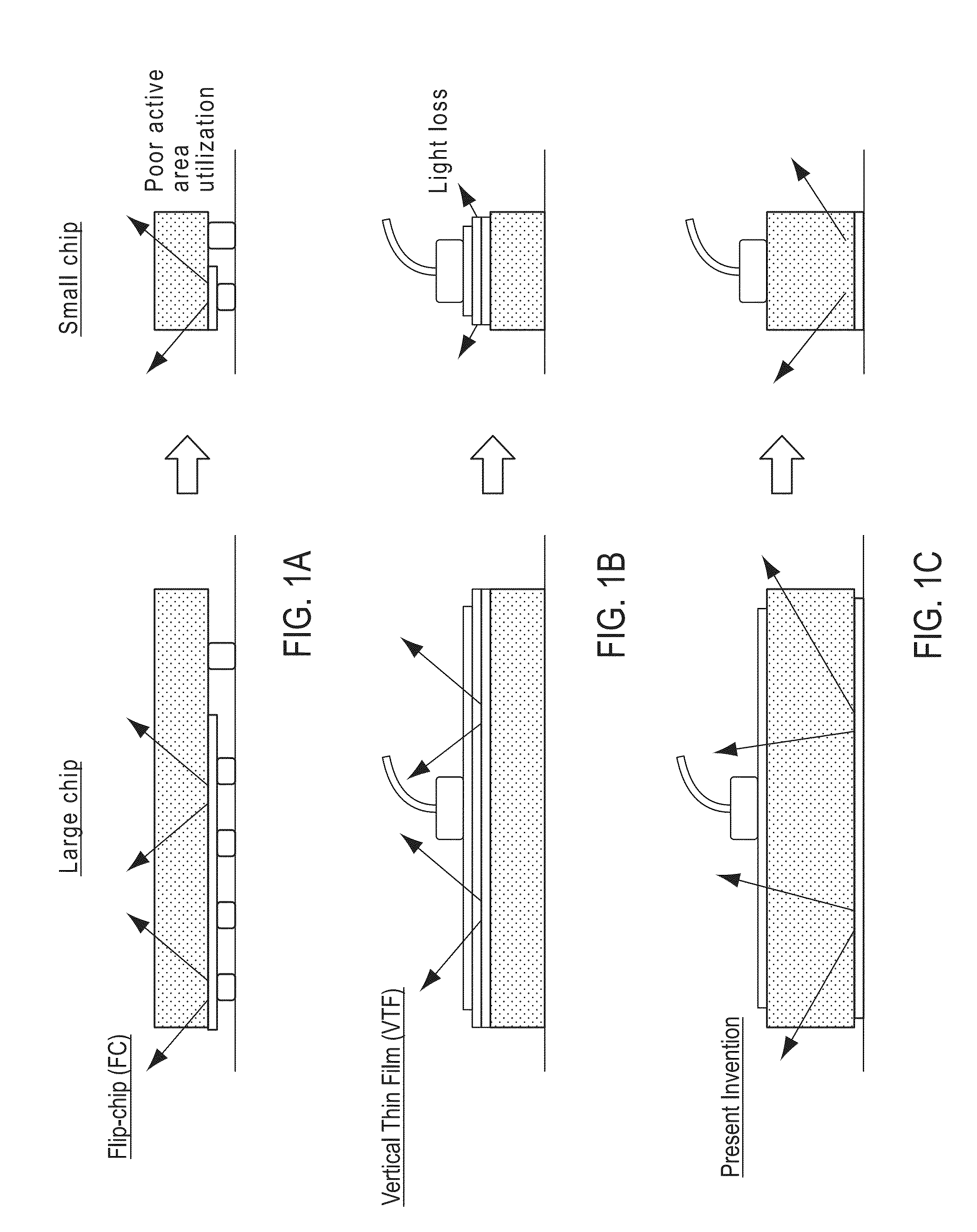
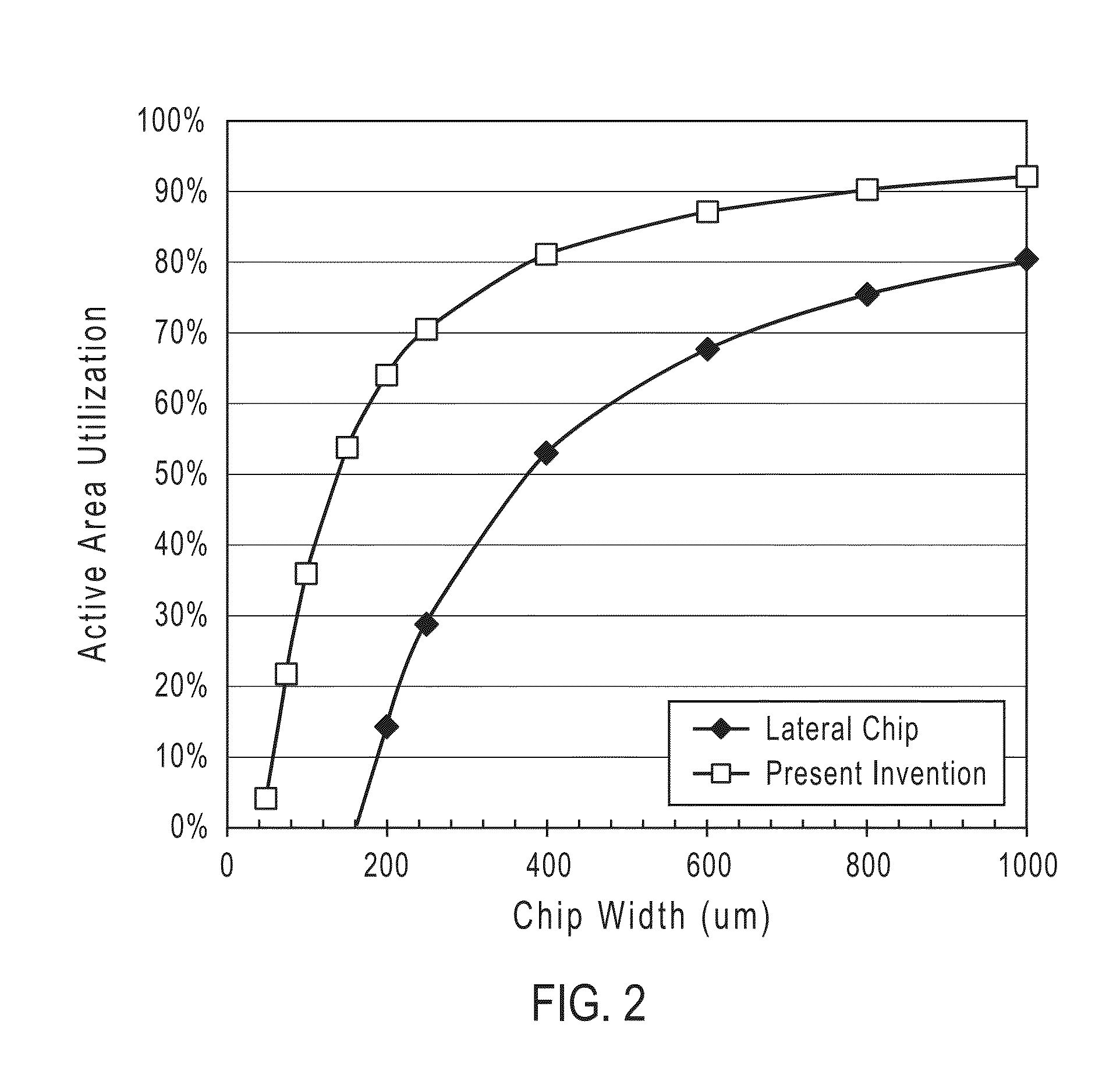
Chip size reduction for lateral chips (either top or substrate emitting) is problematic as fabrication tolerances can reduce active area utilization as chip size is reduced.
This fundamentally reduces active area utilization (portions of the die footprint are required for the cathode) and puts a practical limit on die size.
However, the lattice mismatch between SiC and GaN results in high dislocation densities (>1×108 cm-2) which can cause unreliability at high power densities.
Also, SiC has a higher refractive index than GaN, making the issue of light extraction a more difficult problem.

Method used


Image

  • Power light emitting diode and method with uniform current density operation
  • Power light emitting diode and method with uniform current density operation
  • Power light emitting diode and method with uniform current density operation

Examples


Embodiment Construction

[0053]This invention relates generally to lighting techniques, and in particular to techniques for high current density LED devices fabricated on bulk gallium and nitrogen containing polar, semipolar or nonpolar materials. The invention can be applied to applications such as white lighting, multi-colored lighting, lighting for flat panel displays, other optoelectronic devices, and similar products.

[0054]The disclosure herein relates to making and using a light emitting diode device emitting at a wavelength of 390 nm to 470 nm or at a wavelength of 405 nm to 430 nm. Some of the disclosed embodiments address the desirability of uniform current density across the active region, and some of the device embodiments comprise a bulk gallium and nitrogen containing substrate with a growth to form an active region. Exemplary devices are characterized by having a geometric relationship (e.g., aspect ratio) between a lateral dimension of the device and a vertical dimension of the device such th...


PUM


Abstract

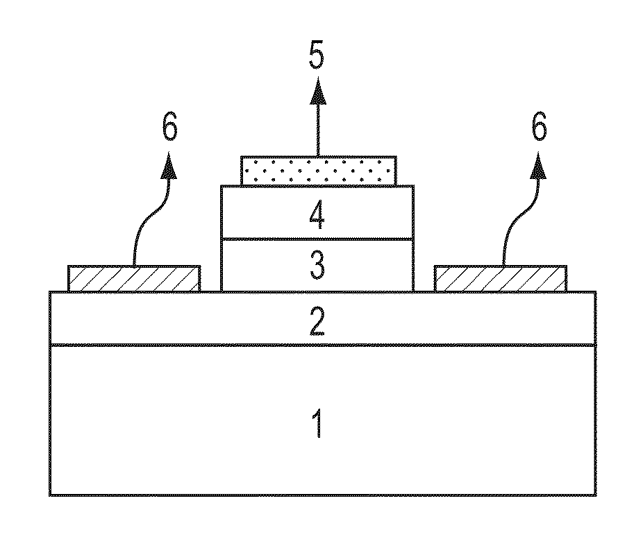
A light emitting diode device has a bulk gallium and nitrogen containing substrate with an active region. The device has a lateral dimension and a thick vertical dimension such that the geometric aspect ratio forms a volumetric diode that delivers a nearly uniform current density across the range of the lateral dimension.

Description

[0001]This application claims the benefit under 35 U.S.C. §119(e) of U.S. Application No. 61 / 778,002 filed on Mar. 12, 2013; and this application is a continuation-in-part of U.S. application Ser. No. 13 / 931,359 filed on Jun. 28, 2013, which is a continuation of U.S. application Ser. No. 12 / 936,238 filed on Jul. 29, 2011, now allowed as U.S. Pat. No. 8,502,465, which claims priority to PCT International Application No. PCT / US2010 / 49531 filed on Sep. 20, 2010, which claims priority to U.S. Provisional Application No. 61 / 243,988, filed on Sep. 18, 2009, each of which is incorporated by reference in its entirety.BACKGROUND[0002]This invention relates generally to lighting techniques, and in particular to techniques for high current density LED devices fabricated on bulk gallium and nitrogen containing polar, semipolar or nonpolar materials. The invention can be applied to applications such as white lighting, multi-colored lighting, lighting for flat panel displays, other optoelectronic...

Claims


Application Information

Patent Timeline
IPC IPC(8): H01L33/02H05B44/00
CPCH01L33/02H01L33/16H01L33/32H01L33/405H01L33/20H05B45/00H01L33/0075
Inventor KATONA, THOMAS M.RARING, JAMES W.D'EVELYN, MARK P.KRAMES, MICHAEL R.DAVID, AURELIEN J.F.
Owner KORRUS INC
Learn More