Methods of manufacturing metal wiring buried flexible substrate by using plasma and flexible substrates manufactured by the same
a technology of flexible substrate and metal wiring, which is applied in the direction of conductive pattern formation, electrical/magnetic/electromagnetic heating, circuit bendability/stretchability, etc., can solve the problems of difficult verification of wiring defect generation during manufacturing process, complex process, and high cost, and achieve low resistance
- Summary
- Abstract
- Description
- Claims
- Application Information
AI Technical Summary
Benefits of technology
Problems solved by technology
Method used
Image

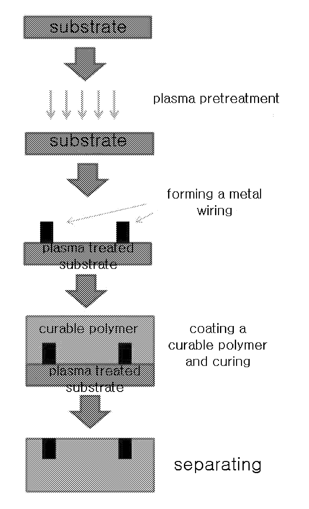


Examples
example 1
Manufacture of a Metal Wiring Buried Flexible Substrate 1
[0051]Step 1: After cleaning a glass substrate using acetone and isopropyl alcohol, a CF4 plasma treatment (process condition; treatment at an CF4 gas of 1 sccm, an Ar gas of 9 sccm, a process pressure of 10 mTorr, and a RF power of 300 W for 300 seconds) was conducted to modify the surface of the substrate to have a hydrophobic property. In this case, the contacting angle of the pre-treated glass substrate with respect to water was 101°.
[0052]Step 2: By using a gravure offset printing apparatus, an Ag paste (silver nano paste DGP, nano new material (ANP)) was coated on she pre-treated glass substrate in Step 1 so form an Ag wiring having a line width of 20 to 500 μm and an interval of 20 to 2,000 μm. The thus formed wiring was heat treated on a hot-plate of 200° C. for 1 hour. After performing the heat treatment, the thickness of the Ag wiring was about 1 to 2 μm.
[0053]Step 3: On the Ag wiring formed in Step 2 and the glass s...
example 2
Manufacture of a Metal Wiring Buried Flexible Substrate 2
[0056]Step 1: After cleaning a glass substrate using acetone and isopropyl alcohol, a CF4 plasma treatment (process condition; treatment at an CF4 gas of 1 sccm, an Ar gas of 9 sccm, a process pressure of 10 mTorr, and an RF power of 300 W for 300 seconds) was conducted to modify the surface of the substrate to have a hydrophobic property. In this case, the contacting angle of the pre-treated glass substrate with respect to water was 101°.
[0057]Step 2: By using a gravure offset printing apparatus, an Ag paste (silver nano paste DGP, nano new material (ANP)) was coated on the pre-treated glass substrate in Step 1 to form an Ag wiring having a line width of 20 to 500 μm and an interval of 20 to 2,000 μm. The thus formed wiring was He plasma treated (process condition; a process pressure or 500 torn, power; 500 W, time period; 10 minutes, temperature; room temperature, electrode rotor number; 1500 rpm, substrate moving velocity; ...
example 3
Manufacture of a Metal Wiring Buried Flexible Substrate 3
[0060]An Ag wiring buried flexible substrate was manufactured by conducting the same procedure explained in Example 1 except for using an STS steel sheet instead of the glass substrate in Step 1 in Example 1. in this case, the contacting angle of the pre-treated STS substrate with respect to water was 107°, and the contacting angle of the STS substrate after the plasma, treatment with respect to water was 82°.
PUM
| Property | Measurement | Unit |
|---|---|---|
| contacting angle | aaaaa | aaaaa |
| contacting angle | aaaaa | aaaaa |
| contacting angle | aaaaa | aaaaa |
Abstract
Description
Claims
Application Information
PatSnap Eureka turns technology decisions into work you can execute. Powered by our Innovation Knowledge Graph, it runs expert workflows across engineering, life sciences, materials and intellectual property. Get your review-ready output in minutes.


