Semiconductor device and method for fabricating the same

a technology of semiconductor devices and semiconductor components, applied in the direction of semiconductor devices, basic electric elements, electrical equipment, etc., can solve the problems of reducing the reliability of semiconductor devices, and achieve the effects of high reliability, stable electrical characteristics, and high reliability of semiconductor devices

Active Publication Date: 2014-02-13
SEMICON ENERGY LAB CO LTD
View PDF8 Cites 70 Cited by
  • Summary
  • Abstract
  • Description
  • Claims
  • Application Information

AI Technical Summary

Benefits of technology

[0014]Since the proportion of indium in the second oxide semiconductor layer is higher than that in each of the first oxide semiconductor layer and the third oxide semiconductor layer, the second oxide semiconductor layer has high carrier mobility and serves as a carrier path. Hence, a carrier flows in a region apart from the oxide insulating layers provided under and over the oxide semiconductor stack. Thus, an effect of impurities or the like entering from the oxide insulating layers can be reduced.
[0016]Further, if silicon or carbon which is one of Group 14 elements is contained as an impurity in the oxide semiconductor layer, it can work as a donor and form an n-type region. Thus, the concentration of silicon contained in the oxide semiconductor layer is made lower than or equal to 3×10¹⁸ atoms / cm3, preferably lower than or equal to 3×10¹⁷ atoms / cm3. Further, the concentration of carbon in the oxide semiconductor layer is made lower than or equal to 3×10¹⁸ atoms / cm3, preferably lower than or equal to 3×10¹⁷ atoms / cm3. It is particularly preferable to employ a structure where the first and the third oxide semiconductor layers sandwich or surround the second oxide semiconductor layer serving as a carrier path so that a large number of Group 14 elements do not enter the second oxide semiconductor layer. That is to say, the first and the third oxide semiconductor layer can also be called barrier layers which prevent Group 14 elements such as silicon from entering the second oxide semiconductor layer.
[0017]If hydrogen or moisture is contained as an impurity in the oxide semiconductor stack, it can work as a donor and form an n-type region. Therefore, in terms of achieving the well-shaped structure, it is useful to provide a protective film (e.g., a silicon nitride film) that prevents entry of hydrogen or moisture from outside, over or under the oxide semiconductor layer.
[0020]In addition to the above-described structure, a first nitride insulating layer may be provided under the first oxide insulating layer, and a second nitride insulating layer may be provided over the second oxide insulating layer. The first and the second nitride insulating layers prevent entry of hydrogen, moisture, or the like into the oxide semiconductor stack.
[0023]For example, the first oxide semiconductor layer, the second oxide semiconductor layer, and the third oxide semiconductor layer are each formed using oxide including indium, zinc, and gallium. When the first oxide semiconductor layer, the second oxide semiconductor layer, and the third oxide semiconductor layer are each formed using the same elements, scatterings at the interface between the first and the second oxide semiconductor layers and the interface between the second and the third oxide semiconductor layers can be reduced.
[0028]According one embodiment of the present invention, it is possible to provide a highly reliable semiconductor device that includes an oxide semiconductor and exhibits stable electrical characteristics. It is possible to fabricate a highly reliable semiconductor device.

Problems solved by technology

Further, entry of an impurity such as hydrogen into the oxide semiconductor layer causes generation of a carrier.
Thus, a shift in electrical characteristics of the transistor occurs, leading to a reduction in reliability of a semiconductor device.

Method used


Image

  • Semiconductor device and method for fabricating the same
  • Semiconductor device and method for fabricating the same
  • Semiconductor device and method for fabricating the same

Examples


embodiment 1

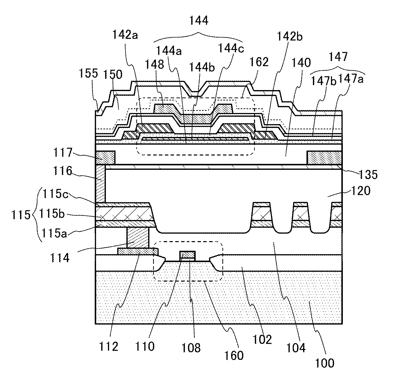
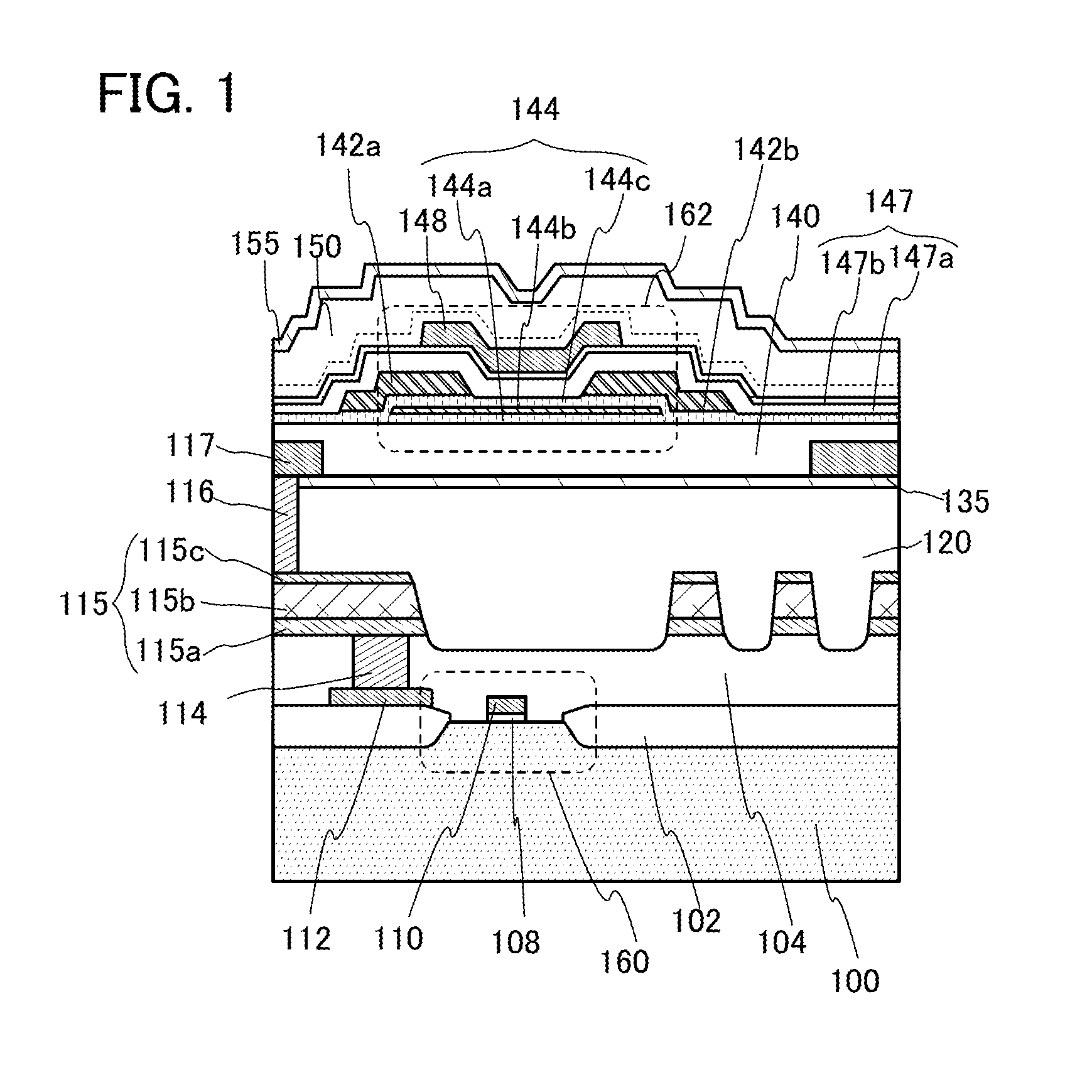
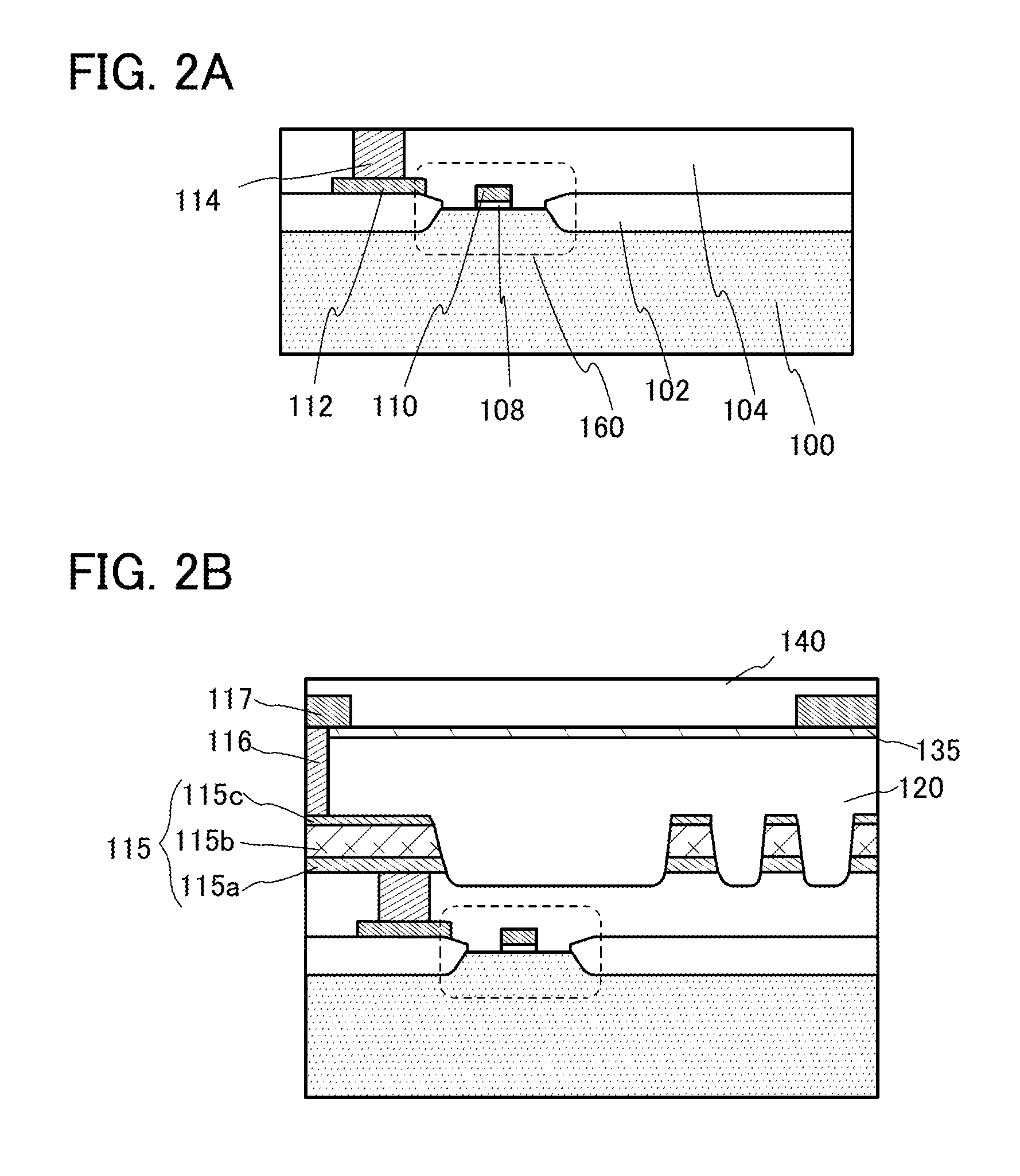
[0050]In this embodiment, a semiconductor device according to one embodiment of the present invention is described in detail with reference to drawings. FIG. 1 illustrates a semiconductor device of one embodiment of the present invention.

[0051]In the semiconductor device, a transistor 160 including a first semiconductor material is formed on a substrate 100, and a transistor 162 including a second semiconductor material is formed over the transistor 160.

[0052]Here, the semiconductor materials included in the transistor 160 and the transistor 162 preferably have different band gaps. For example, a silicon-based semiconductor (single crystal silicon, polycrystalline silicon, or the like) can be used for the first semiconductor material, and an oxide semiconductor can be used for the second semiconductor material. A transistor including a silicon-based semiconductor can easily operate at high speed. A transistor including an oxide semiconductor, on the other hand, has low off-state cur...

embodiment 2

[0181]FIG. 6A illustrates an example of a circuit diagram of a NOR circuit, which is a logic circuit, as an example of the semiconductor device described in Embodiment 1. FIG. 6B is a circuit diagram of a NAND circuit.

[0182]In the NOR circuit illustrated in FIG. 6A, p-channel transistors 801 and 802 each have a structure similar to that of the transistor 160 in FIG. 1 in that a single crystal silicon substrate is used for the channel formation region, and n-channel transistors 803 and 804 each have a structure similar to structures of the transistor 162 illustrated in FIG. 1, the transistors 163 and 164 illustrated in FIGS. 4A and 4B, and the transistors 172 to 174 illustrated in FIGS. 5A to 5C in that an oxide semiconductor film is used for the channel formation region.

[0183]In the NOR circuit illustrated in FIG. 6A, a conductive layer controlling electrical characteristics of the transistor may be provided to overlap with a gate electrode layer with an oxide semiconductor film pro...

embodiment 3

[0191]In this embodiment, an example of a semiconductor device (memory device) which includes the semiconductor device described in Embodiment 1, which can hold stored data even when not powered, and which has an unlimited number of write cycles is described with reference to drawings.

[0192]FIG. 7A is a circuit diagram illustrating the semiconductor device of this embodiment.

[0193]A transistor 260 illustrated in FIG. 7A can have a structure similar to that of the transistor 160 illustrated in FIG. 1 and easily operates at high speed. Further, a transistor 262 can have a structure similar to structures of the transistor 162 illustrated in FIG. 1, the transistors 163 and 164 illustrated in FIGS. 4A and 4B, and the transistors 172 to 174 illustrated in FIGS. 5A to 5C and enables charge to be held for a long time owing to its characteristics.

[0194]Although all the transistors are n-channel transistors here, p-channel transistors can be used as the transistors used for the semiconductor ...


PUM


Abstract

To provide a highly reliable semiconductor device exhibiting stable electrical characteristics. To fabricate a highly reliable semiconductor device. Included are an oxide semiconductor stack in which a first to a third oxide semiconductor layers are stacked, a source and a drain electrode layers contacting the oxide semiconductor stack, a gate electrode layer overlapping with the oxide semiconductor layer with a gate insulating layer provided therebetween, and a first and a second oxide insulating layers between which the oxide semiconductor stack is sandwiched. The first to the third oxide semiconductor layers each contain indium, gallium, and zinc. The proportion of indium in the second oxide semiconductor layer is higher than that in each of the first and the third oxide semiconductor layers. The first and the third oxide semiconductor layers are each an amorphous semiconductor film. The second oxide semiconductor layer is a crystalline semiconductor film.

Description

BACKGROUND OF THE INVENTION[0001]1. Field of the Invention[0002]The present invention relates to a semiconductor device and a method for fabricating the semiconductor device.[0003]Note that a semiconductor device in this specification refers to all devices which can function by utilizing semiconductor characteristics, and electro-optical devices, semiconductor circuits, and electronic devices are all semiconductor devices.[0004]2. Description of the Related Art[0005]Attention has been focused on a technique for forming a transistor including a semiconductor thin film formed over a substrate having an insulating surface (also referred to as a thin film transistor). The transistor is applied to a wide range of electronic devices such as an integrated circuit (IC) or an image display device (display device). A silicon-based semiconductor material is widely known as a material for a semiconductor thin film applicable to a transistor. As another material, an oxide semiconductor has been ...

Claims


Application Information

Patent Timeline
Patent Type & Authority Applications(United States)
IPC IPC(8): H01L29/267
CPCH01L29/267H01L27/11807H01L27/1225H10B12/05H10B41/70H01L21/31051H01L21/324H01L29/1054H01L29/4908H01L29/66742
Inventor YAMAZAKI, SHUNPEI
Owner SEMICON ENERGY LAB CO LTD
Why Eureka
Try Eureka