
Method and system for determining overlap process windows in semiconductors by inspection techniques

a technology of overlap process and inspection technique, applied in semiconductor/solid-state device testing/measurement, instruments, photomechanical equipment, etc., can solve problems such as uncertainty in overlaying the image of the pattern of the current material layer, affecting the accuracy of alignment, so as to reduce the overall effort and fast response time

Inactive Publication Date: 2014-03-06
GLOBALFOUNDRIES US INC
View PDF1 Cites 7 Cited by
  • Summary
  • Abstract
  • Description
  • Claims
  • Application Information

AI Technical Summary

Benefits of technology

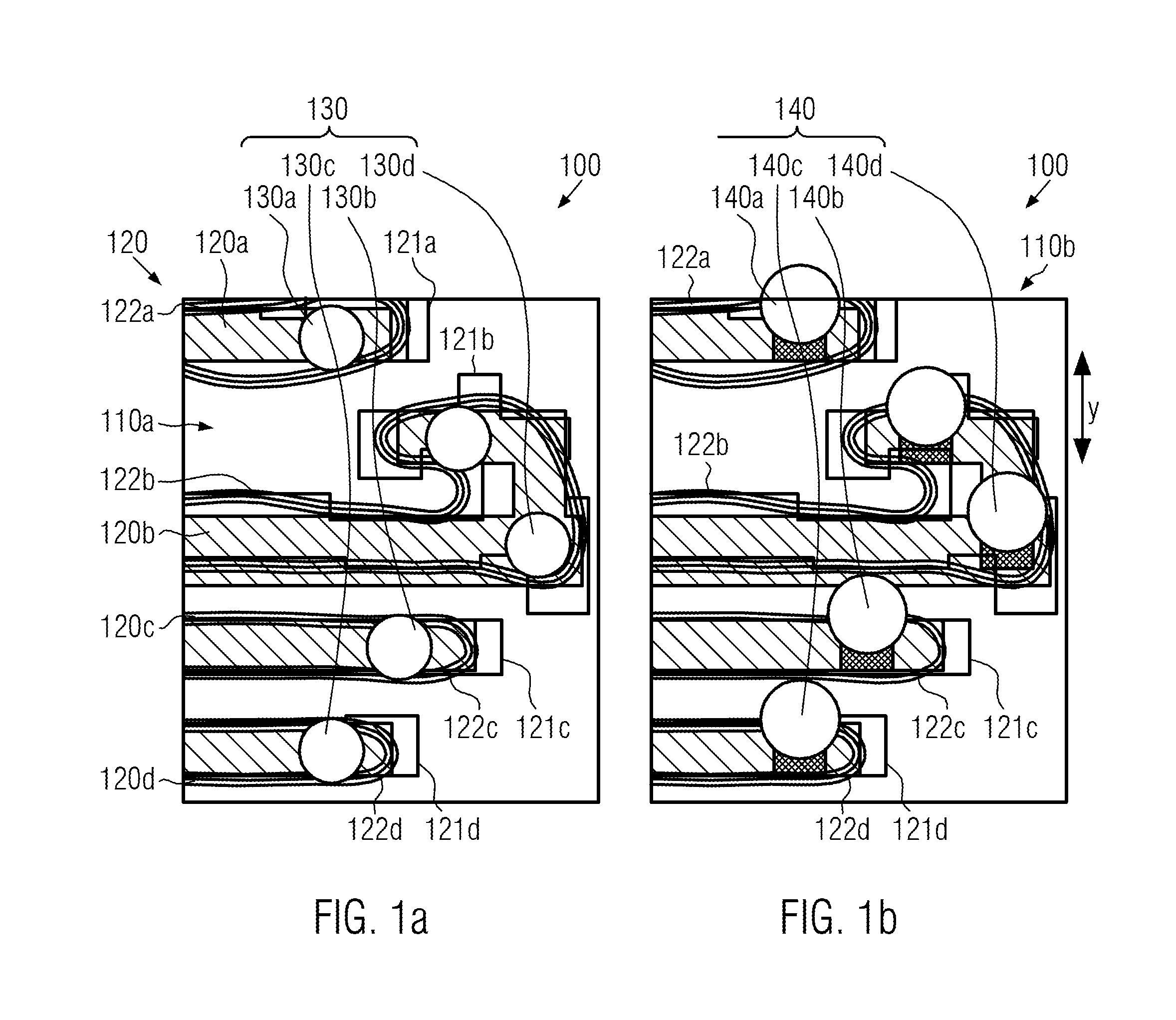
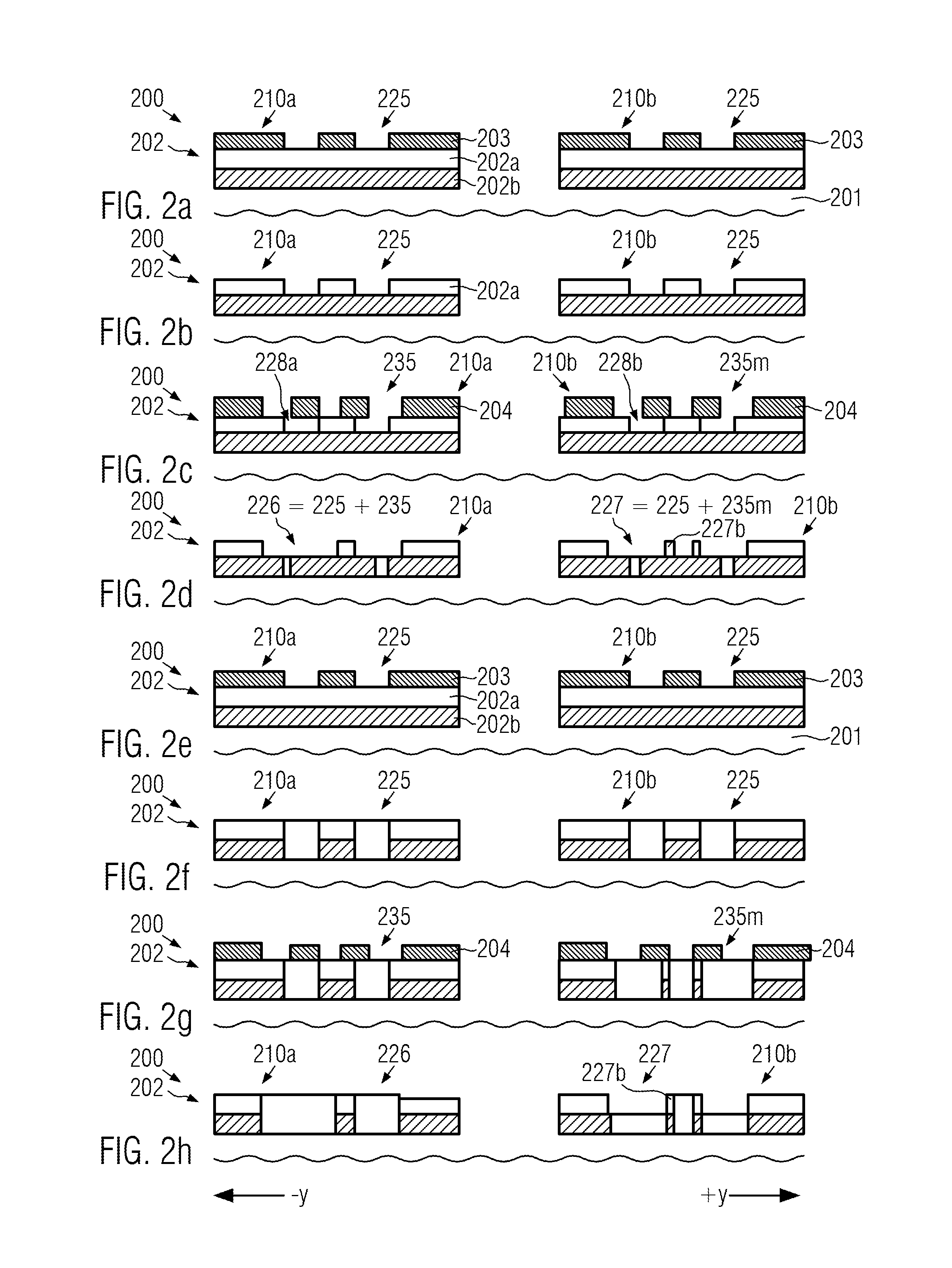
The present patent provides techniques and systems for efficiently identifying areas of a semiconductor device that are critical for overlay accuracy and can result in failures. By using existing detection methods, such as defect detection or inspection, the areas can be examined without requiring expensive cross-sectional analysis. This allows for faster response times and reduces overall effort compared to conventional strategies. One method involves transferring patterns from two layout layers into a material layer to define an overlap area and assessing process margin. Another method involves transferring a geometrically modulated version of one pattern into the material layer. Overall, this patent provides more efficient and effective ways to identify and improve upon critical areas of semiconductor devices.

Problems solved by technology

These registration tolerances are caused by, for example, a variation of a photoresist image on the substrate due to non-uniformities in such parameters as resist thickness, baking temperature, exposure dose and time and development conditions.
Furthermore, non-uniformities of the etch processes can also lead to variations of the etched features.
In addition, there exists an uncertainty in overlaying the image of the pattern of the current material layer to the etched or otherwise defined pattern of the previously formed material layer while photolithographically transferring the image of the photo mask onto the substrate.
Several factors contribute to an imperfect ability of the imaging system to overlay two layers, such as imperfections within a set of masks, temperature differences at the different times of exposure, a limited registration capability of the alignment tool and, as a major contribution to alignment errors, imperfections of the exposure tool itself, such as lens distortions, and distortions caused by the alignment hardware, such as the substrate holder, and the like.
The situation becomes even worse when different exposure tools are used for defining subsequent device layers, since then the inherent errors in the exposure tool and related components may vary between the different tools.
Although the same exposure tool might be used for imaging critical device layers, in practice, such restrictions may not allow an efficient overall process flow in a complex manufacturing environment, which typically comprises a plurality of lithography tools for the same device layer.
For example, when forming a wiring structure for an integrated circuit, respective metal lines and vias, which connect two stacked metal regions, may have to be aligned to each other with strict process margins so as to result in a well-defined overlap, since a significant misalignment may cause a short between actually non-connected lines, thereby possibly creating a fatal device defect, while a reduction of the intended overlap area may cause loss of performance due to increased contact and series resistance.
During the lithography process and subsequent etch processes, however, significant changes of the initial layout pattern may be caused, for instance, by thinning small structures and the like.
As discussed above, the various process steps involved in actually forming a desired pattern in a material layer of the semiconductor device may result in a more or less pronounced introduction of process imperfections, for instance, non-perfect alignment of the lithography mask to the semiconductor substrate, process tolerances caused by the imaging process such as lens aberrations and distortions of the substrate by mechanical stress and the like, and also various tolerances during the etch processes may result in inaccuracies of the resulting device patterns, which in turn may thus result in a reduced overlay accuracy.
Although an increased degree of process robustness may be accomplished by using, for example, optical proximity correction techniques, it is nevertheless very difficult to identify the most critical overlap areas since at least two subsequent pattern transfer processes are involved so that a number of possible sources for generating overlay errors may be quite high so as to predict any such process variations by corresponding models used for OPC strategies.
On the other hand, a direct observation of critical overlap areas is very difficult, since the underlying layer may not be accessible by well-established inspection techniques, such as scanning electron microscopy.
In other strategies, overlay performance is measured on the basis of electrical measurement procedures, for instance by forming contact chains and using contacts with a specified degree of “misalignment.” This approach, however, is restricted to special structures and locations inside the image field or chip area.
In other cases, yield measurement data may be used for identifying critical overlap areas wherein, however, a direct influence of critical overlap areas on the resulting final production yield is difficult to determine unless corresponding misalignments may be determined on the basis of cross-sectional electron microscopy measurements which, however, are very expensive due to the cross-sectional preparation of the samples.
Furthermore, this strategy results in a very long response time so that identification of critical overlap areas may still result in significant yield loss due to a large number of inappropriately processed substrates.
Furthermore, as discussed above, any algorithms to identify critical overlap structures in the basic semiconductor design may still require confirmation on substrate level and may not appropriately accommodate various process imperfections.

Method used


Image

  • Method and system for determining overlap process windows in semiconductors by inspection techniques
  • Method and system for determining overlap process windows in semiconductors by inspection techniques
  • Method and system for determining overlap process windows in semiconductors by inspection techniques

Examples


Embodiment Construction

[0023]Various illustrative embodiments of the invention are described below. In the interest of clarity, not all features of an actual implementation are described in this specification. It will of course be appreciated that in the development of any such actual embodiment, numerous implementation-specific decisions must be made to achieve the developers' specific goals, such as compliance with system-related and business-related constraints, which will vary from one implementation to another. Moreover, it will be appreciated that such a development effort might be complex and time-consuming, but would nevertheless be a routine undertaking for those of ordinary skill in the art having the benefit of this disclosure.

[0024]The present subject matter will now be described with reference to the attached figures. Various structures, systems and devices are schematically depicted in the drawings for purposes of explanation only and so as to not obscure the present disclosure with details ...


PUM


Abstract

The formation of overlap areas in sophisticated semiconductor devices is a critical aspect which may not be efficiently evaluated on the basis of conventional measurement and design strategies. For this reason, the present disclosure provides measurement techniques and systems in which overlying device patterns are transformed into the same material layer, thereby forming a combined pattern which is accessible by well-established defect inspection techniques. Upon geometrically modulating some of these combined patterns, a systematic evaluation of overlap process windows may be accomplished.

Description

BACKGROUND OF THE INVENTION[0001]1. Field of the Invention[0002]The present disclosure generally relates to the field of fabricating microstructures, such as integrated circuits, and, more particularly, to a technique for determining alignment accuracy and pattern placement precision during patterning processes.[0003]2. Description of the Related Art[0004]The fabrication of microstructures, such as integrated circuits, requires tiny regions of precisely controlled size to be formed in a material layer of an appropriate substrate, such as a silicon substrate, a silicon-on-insulator (SOI) substrate, or other suitable carrier materials. These tiny regions of precisely controlled size are generated by patterning the material layer using lithography, etch, implantation, deposition, oxidation processes and the like, wherein typically, at least in a certain stage of the patterning process, a mask layer may be formed over the material layer to be treated to define these tiny regions. Genera...

Claims


Application Information

Patent Timeline
IPC IPC(8): H01L21/66G01N23/00
CPCH01L21/67288H01L22/12G03F7/70633G03F7/7065G03F7/70683G03F1/70G03F7/20H01L21/027H01L21/0274H01L22/30
Inventor BAUCH, LOTHAR
Owner GLOBALFOUNDRIES US INC
Learn More