Cleaning composition and method for cleaning a semiconductor device substrate after chemical mechanical polishing
- Summary
- Abstract
- Description
- Claims
- Application Information
AI Technical Summary
Benefits of technology
Problems solved by technology
Method used
Image

Examples
examples
[0034]All chemicals used for preparing the examples which follow are commercially available unless otherwise mentioned. A commercial alkaline copper post-CMP cleaner, EKC™ PCMP5600, (available from EKC Technology, Inc.) was used as a reference solution.
[0035]Further, unless expressly stated to the contrary, “or” refers to an inclusive or and not to an exclusive or. For example, a condition A or B is satisfied by any one of the following: A is true (or present) and B is false (or not present), A is false (or not present) and B is true (or present), and both A and B are true (or present).
[0036]Unless expressly stated otherwise, the term “about” as used herein is intended to include and take into account variations due to manufacturing tolerances and / or variabilities in process control.
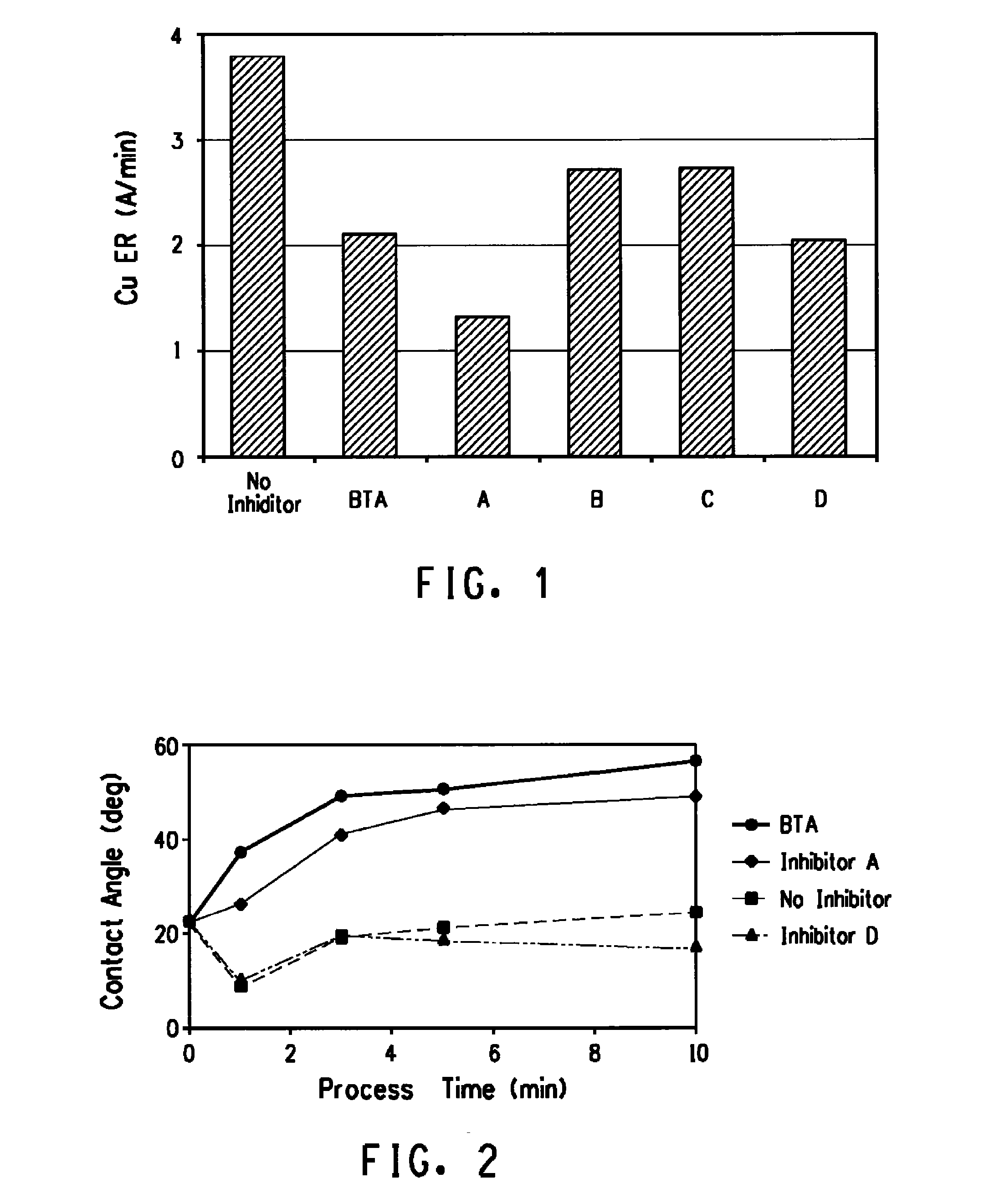
Copper Etch Rate
[0037]Copper thickness was measured for the test samples using an automated sheet resistivity meter, 280P (Four Dimensions, Inc.). Copper etch rates of each test solution were calculated ...
PUM
 Abstract
Description
Claims
Application Information
 - Generate Ideas
- Intellectual Property
- Life Sciences
- Materials
- Tech Scout
- Unparalleled Data Quality
- Higher Quality Content
- 60% Fewer Hallucinations
Browse by: Latest US Patents, China's latest patents, Technical Efficacy Thesaurus, Application Domain, Technology Topic, Popular Technical Reports.
© 2025 PatSnap. All rights reserved.Legal|Privacy policy|Modern Slavery Act Transparency Statement|Sitemap|About US| Contact US: help@patsnap.com