UV Irradiation Apparatus with Cleaning Mechanism and Method for Cleaning UV Irradiation Apparatus

a technology of irradiation apparatus and cleaning mechanism, which is applied in the direction of spraying apparatus, chemistry apparatus and processes, coatings, etc., can solve the problems of reducing mechanical strength, elastic modulus, and low dielectric constant, and achieve the effect of efficient implementation of such cleaning methods

Inactive Publication Date: 2014-05-01
ASM IP HLDG BV
View PDF6 Cites 372 Cited by
  • Summary
  • Abstract
  • Description
  • Claims
  • Application Information

AI Technical Summary

Benefits of technology

[0011]In an embodiment of the present invention, a step to clean the UV transmission window and inner walls of the UV irradiation chamber is provided, as a cleaning method for UV irradiation chamber, whereby UV light that has passed through the UV transmission window in the UV irradiation chamber is irradiated onto the substrate, after which the auxiliary RF electrodes in the chamber are used to generate active species. A UV irradiation apparatus comprising a cleaning mechanism to efficiently implement such cleaning method is also provided. In an embodiment, this cleaning method may be combined with the conventional O2+UV ozone cleaning. In another embodiment of the present invention, a more efficient cleaning method is presented, whereby cleaning gas that contains fluorine instead of or in addition to O2 under the aforementioned method is used to generate active species through the auxiliary RF electrodes provided in the chamber. In such case, in an embodiment a material which offers a transmission ratio high enough not to let the light transmission window corrode due to fluorine is selected. For this material, CaF2, MgF2, BaF2, Al2O3 or other crystal, or synthetic quartz coated with CaF2, MgF2, BaF2 or Al2O3, can be used.

Problems solved by technology

Low-k (low dielectric constant film) materials are used to reduce the inter-layer volume, but these materials not only lower the dielectric constant, but they also reduce the mechanical strength (EM: elastic modulus) and are vulnerable to stress received after the CMP, wire bonding, and packaging post-processes.
However, UV light generating high energy presents problems, such as a lower transmission ratio that is likely to occur due to the material of the light transmission window and the attachment of deposits on the window material, and a shorter maintenance cycle (the light transmission window must be cleaned or replaced frequently or at very short intervals) in curing processes where a large amount of outgas (decomposition gas that produces film on the irradiation target) generates.
However, this method requires a large, expensive apparatus and thus, an inexpensive, space-saving method is desired.

Method used


Image

  • UV Irradiation Apparatus with Cleaning Mechanism and Method for Cleaning UV Irradiation Apparatus
  • UV Irradiation Apparatus with Cleaning Mechanism and Method for Cleaning UV Irradiation Apparatus
  • UV Irradiation Apparatus with Cleaning Mechanism and Method for Cleaning UV Irradiation Apparatus

Examples


example 1

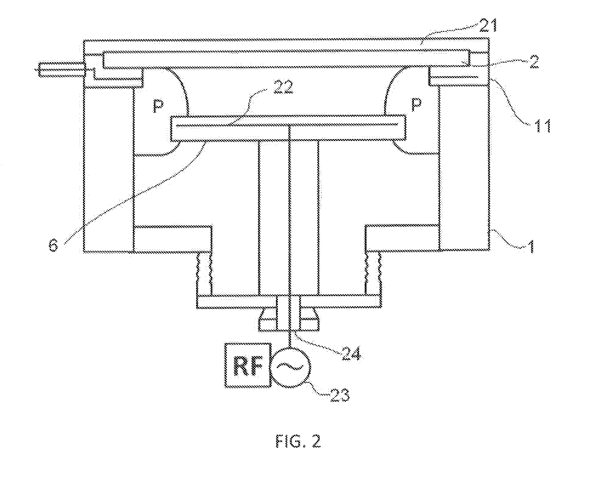
[0075]A substrate (300 mm in diameter) having a dielectric film containing a porogen material formed thereon was loaded in a UV irradiation apparatus illustrated in FIG. 2 provided with a transmission window made of synthetic quartz (SiO2) having a thickness of 20 mm. The dielectric film formed on the substrate was cured in the apparatus under the following conditions:[0076]Pressure: 1-50 Torr[0077]Supplied gas: Nitrogen gas[0078]Temperature: 300-450° C.[0079]Distance between the substrate and the lamps: 5-350 mm[0080]UV wavelength: 150-400 nm[0081]Illuminance (output or intensity) of UV lamps: 5-200 W / cm2 [0082]Irradiation duration: 60 to 600 seconds

[0083]UV transmittance (%) of the transmission window (“a” in FIG. 7) was measured using a spectrophotometer prior to the curing. After 20 substrates were cured, UV transmittance (%) of the transmission window (“b” in FIG. 7) was again measured using a spectrophotometer.

[0084]Next, the reaction chamber was subjected to cleaning. The cle...

example 2

[0092]The same tests as in Example 1 were conducted except that the transmission window made of synthetic quartz was coated by a layer of Al2O3 having a thickness of 300 nm.

[0093]The results are shown in FIG. 8 which is a graph showing the relationships between UV transmittance (%) and wavelength (nm). As shown in FIG. 8, after the UV curing, UV transmittance of the transmission window decreased (“f”) as compared with the initial UV transmittance of the transmission window (“e”) regardless of the wavelength of UV light. When the cleaning gas was O2, UV transmittance was recovered substantially to the initial degree by the cleaning (“f”). Also when the cleaning gas was NF3, UV transmittance was recovered almost to the initial degree by the cleaning (“h”). By visual inspection, no roughness or cloudiness was observed on the surface of the transmission window when the cleaning gas was NF3. Thus, when the surface of the transmission window coated with Al2O3 has resistance against corros...

example 3

[0094]For evaluating cleaning rate, three wafer coupons were attached to a lower surface of a gas ring at positions illustrated in FIG. 9 which is a schematic top cross sectional view of the gas ring, wherein numbers in circles are coupon numbers (the coupon numbers are indicated on the gas ring for illustrative purposes, and the coupons were attached on a lower surface of the gas ring which is not shown in FIG. 9). The gas ring 11 included a circular gas channel 91 provided with a gas inlet port 90 and having gas nozzles 92 extending from the circular gas channel in a radical direction toward the center. Coupon No. 3 was attached near an exhaust, and coupon No. 1 was attached opposite to coupon No. 3. Coupon No. 2 was attached between coupon No. 1 and No. 3. The coupon had a film constituted by Si, O, C, and H, and by cleaning, carbon in the film was removed from the film, thereby reducing the thickness of the film. When the reduction degree of the film thickness was high, the cont...


PUM

PropertyMeasurementUnit
wavelengthaaaaaaaaaa
thicknessaaaaaaaaaa

Abstract

A UV irradiation apparatus for processing a semiconductor substrate includes: a UV lamp unit; a reaction chamber disposed under the UV lamp unit; a gas ring with nozzles serving as a first electrode between the UV lamp unit and the reaction chamber; a transmission window supported by the gas ring; an RF shield which covers a surface of the transmission window facing the UV lamp unit; a second electrode disposed in the reaction chamber for generating a plasma between the first and second electrodes; and an RF power source for supplying RF power to one of the first or second electrode.

Description

BACKGROUND[0001]1. Field of the Invention[0002]The present invention generally relates to a UV irradiation apparatus for processing a substrate such as a semiconductor wafer using UV light and a method for cleaning the UV irradiation apparatus, particularly, cleaning a transmission window and an inner wall of the apparatus.[0003]2. Description of the Related Art[0004]In general, UV irradiation apparatuses have been used for the quality modification of various processing targets via ultraviolet light and preparation of substances using photochemical reaction. With the recent trend for higher integration of devices, which requires finer wiring designs and multi-layer wiring structures, it is essential to reduce the inter-layer volume to make the devices operate faster while consuming less power. Low-k (low dielectric constant film) materials are used to reduce the inter-layer volume, but these materials not only lower the dielectric constant, but they also reduce the mechanical streng...

Claims


Application Information

Patent Timeline
Patent Type & Authority Applications(United States)
IPC IPC(8): H01L21/02
CPCH01L21/02H01L21/67115H01L21/02348C23C16/4405C23C16/482B08B7/0057H01J37/32862
Inventor TSUJI, NAOTOFUKASAWA, YASUSHI
Owner ASM IP HLDG BV
Why Eureka
Try Eureka