

Method for Bonding Substrates, Method for Maufaturing Sealing Structure, and Method for Maufaturing Light-Emitting Device
- Summary
- Abstract
- Description
- Claims
- Application Information
AI Technical Summary
Benefits of technology
Problems solved by technology
Method used
Image

Examples
embodiment 1
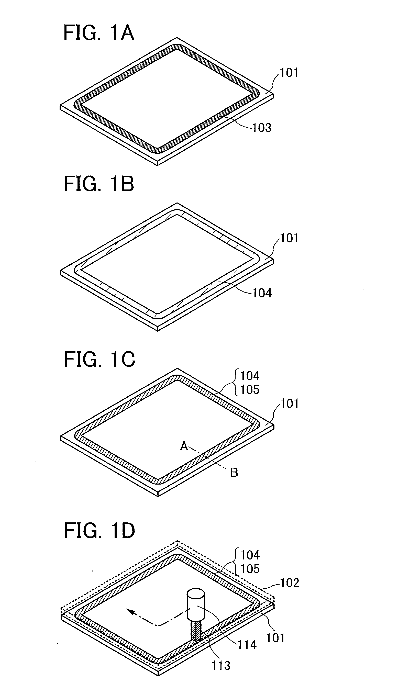
[0046]In this embodiment, a method for bonding substrates which is one embodiment of the present invention and a manufacturing method of a sealing structure using the method for bonding are described.
[0047]First, a frit paste 103 including glass frit is formed as a pattern over a first substrate 101 (FIG. 1A). Here, the frit paste 103 is formed as a pattern to have a closed curve along the outer periphery of the first substrate 101.
[0048]Note that in the case where the first substrate 101 and a second substrate 102 described later are only simply bonded, that is, in the case where a sealed region surrounded by these two substrates and a glass layer does not need to be formed, the frit paste 103 does not need to be formed as a pattern to have a closed curve and may be formed over only a bonding portion.
[0049]The frit paste 103 includes at least glass frit including low-melting-point glass and a binder. The binder includes an organic resin or an organic solvent. Further, the frit past...
embodiment 2
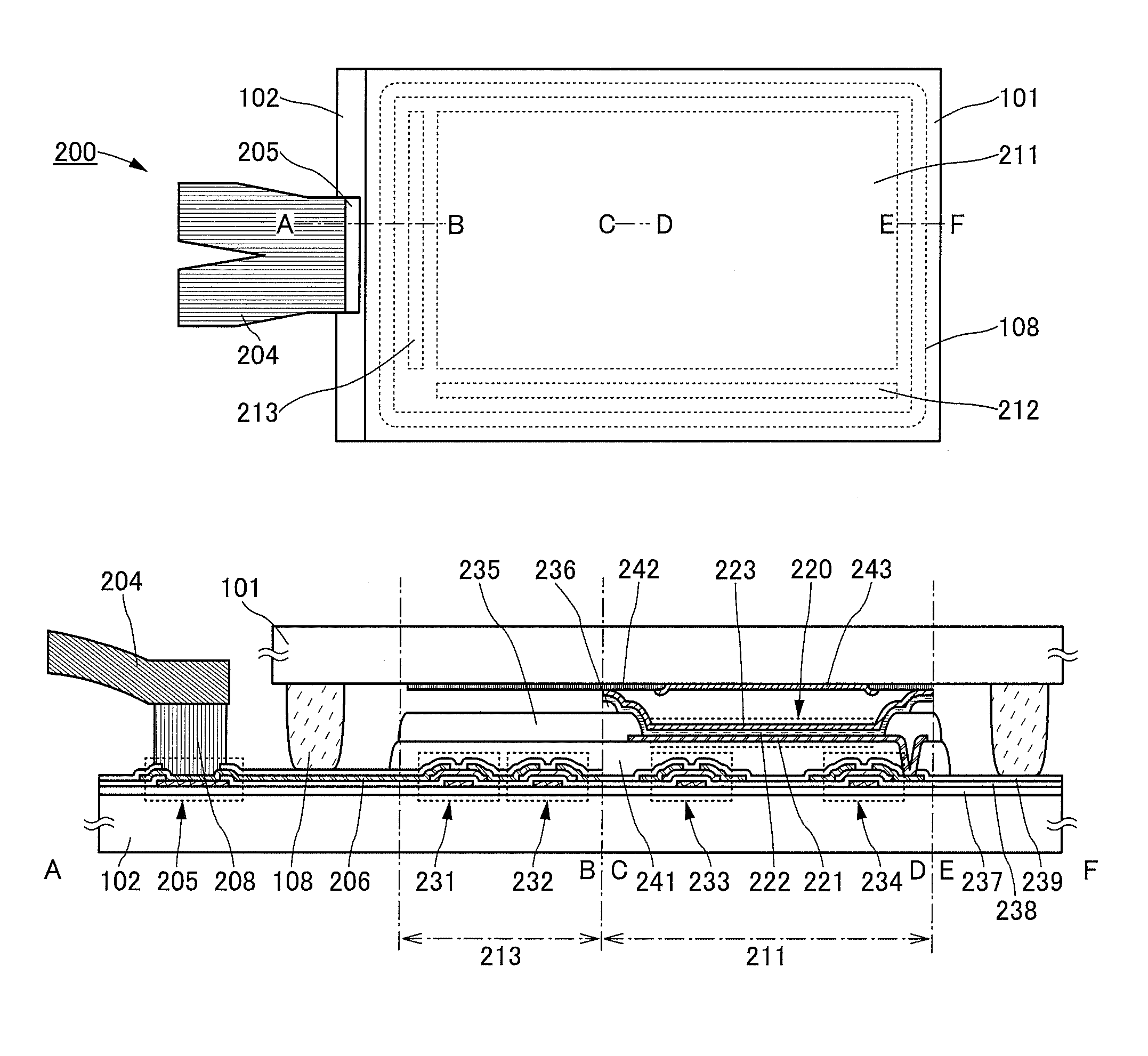
[0112]In this embodiment, an example of a method for manufacturing a light-emitting device using the method for bonding which is one embodiment of the present invention is described. Note that description of the portions already described in Embodiment 1 is omitted or is simplified.
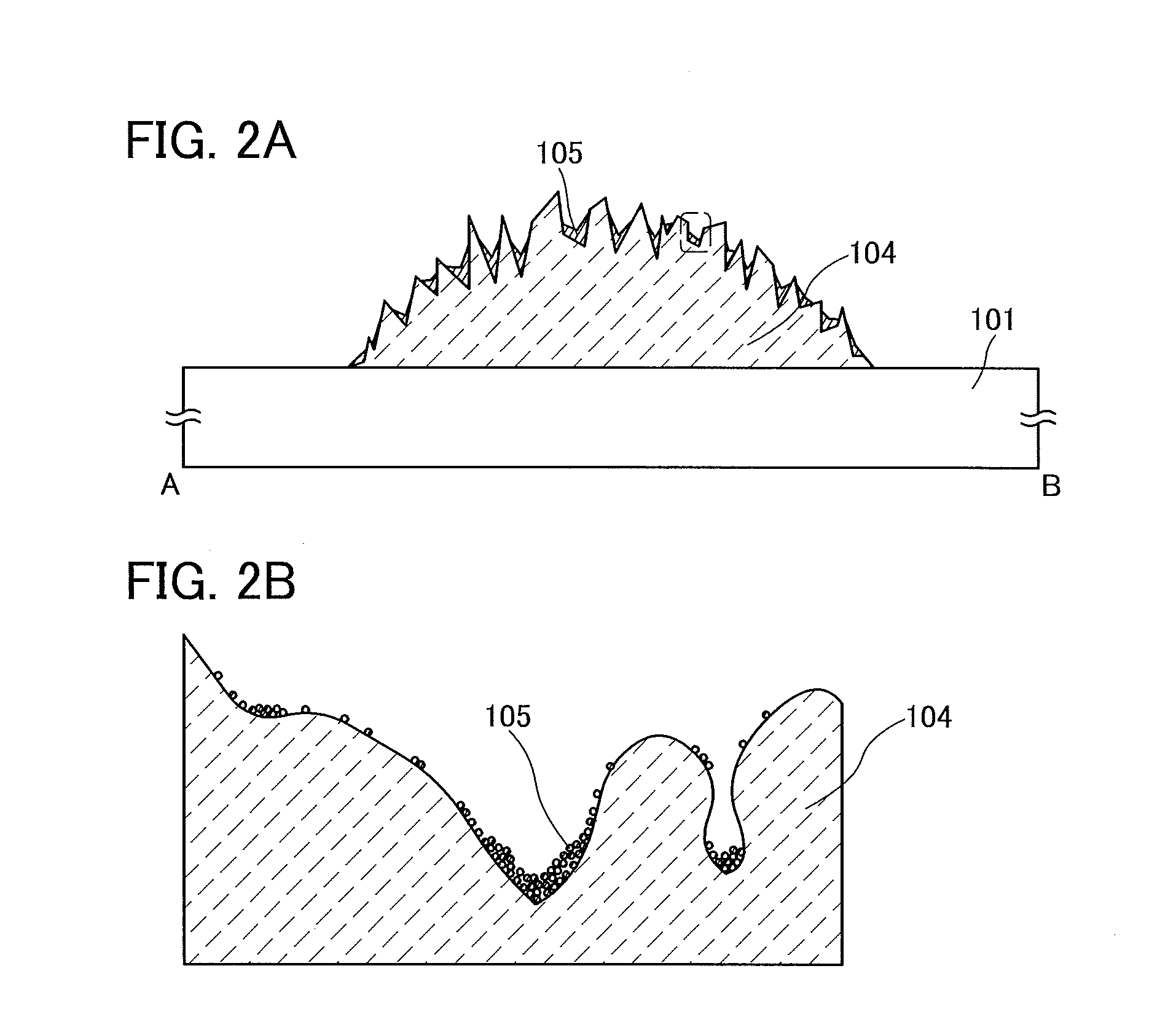
[0113]First, as in Embodiment 1, after the frit paste 103 is formed as a pattern over the first substrate 101, the frit paste 103 is heated to form the glass layer 104 (FIG. 6A).
[0114]Next, a color filter 121 is formed in a region surrounded by the glass layer 104 over the first substrate 101. At the same time, the light-absorbing material 105 is formed over the glass layer 104 (FIG. 6B).
[0115]As the color filter 121, a resin including the particles with a light absorbing property described in Embodiment 1 as a pigment can be used.
[0116]As a method for framing the color filter 121, for example, an etching method, a color resist method, and the like are given.
[0117]In the case where color filters having di...
embodiment 3
[0130]A sealing structure to which the method for bonding substrates which is one embodiment of the present invention is applied has significantly high airtightness, and thus can be used in various devices including an element such as an organic EL element, an organic semiconductor element, or an organic solar cell, whose performance is rapidly decreased once the element is exposed to the air (including moisture or oxygen). Further, the method for forming a sealing structure which is one embodiment of the present invention can be also used for devices having low heat resistance and the above-described various devices can be manufactured with high productivity.
[0131]As a light-emitting device including an organic EL element, a display device, a lighting device, or the like can be given. As a display device including an organic EL element, a display device employing a passive matrix mode (i.e., simple matrix mode) or an active matrix mode can be given. A structural example of a displa...
PUM
| Property | Measurement | Unit |
|---|---|---|
| Shape | aaaaa | aaaaa |
| Light | aaaaa | aaaaa |
Abstract
Description
Claims
Application Information