Micro lens array substrate, electro-optical device, and electronic apparatus

a technology of micro lens array and substrate, applied in the field of micro lens array substrate, can solve the problems of reducing affecting the efficiency of light utilization, so as to suppress the effect of unnecessary reflection or scattering of light at the interface of discontinuous parts, reducing the transmittance of incident light, and improving heat resistan

Active Publication Date: 2014-05-01
SEIKO EPSON CORP
View PDF5 Cites 8 Cited by
  • Summary
  • Abstract
  • Description
  • Claims
  • Application Information

AI Technical Summary

Benefits of technology

[0010]In this case, a stress being applied to the lens layer is distributed because the discontinuous part is provided between the adjacent concave portions in the third direction among the first direction, the second direction and the third direction in the lens layer that is formed in such a manner as to fill in the concave portion in the substrate and to cover the region where the concave portion is formed. Furthermore, because a volume of the entire lens layer is decreased by as much as a space occupied by the discontinuous part, the stress being applied to the lens layer is alleviated. On the other hand, because the lens layer is continuous between the adjacent concave portions in at least one of the first direction and the second direction and light incident on a space between the micro lenses is gathered by the micro lens and thus is utilized, the efficiency of utilization of light is improved, compared to a case where the micro lenses are arranged with spacing in between. Because of this, the crack in the lens layer is suppressed, and additionally, the micro lens array substrate capable of improving the efficiency of utilization of light can be provided.Application Example 2
[0023]In this case, the electro-optical device is equipped with the micro lens array substrate that suppresses the crack in the lens layer and additionally improves the efficiency of utilization of light. This makes it possible to provide the liquid crystal device that is high in quality and is bright in display.Application Example 8
[0027]In this case, the concave portions that are partitioned into the shape of a lattice are formed on the one surface of the substrate and the lens layer is formed in such a manner as to fill in the concave portions in the one surface of the substrate and to cover the region where the concave portions are formed. Thereafter, the part in which the substrate is exposed is formed in the position that overlaps the four corners of the each of the regions that are partitioned in the shape of a lattice, by stripping off the one part of the lens layer. For this reason because the part of the lens layer, in which the substrate is exposed, is a discontinuous part, the stress applied to the lens layer is distributed. Furthermore, because the volume of the entire lens layer is decreased by as much as a space occupied by the stripped-off one part, the stress being applied to the lens layer can be alleviated. On the other hand, because in positions other than the positions that correspond to the four corners of each of the regions that are partitioned into the shape of a lattice, the lens layer is continuous and light that enters a space between the micro lenses is gathered by the micro lens and thus is utilized, the efficiency of utilization of light can be improved. Because of this, the crack in the lens layer is suppressed, and additionally, the micro lens array substrate capable of improving the efficiency of utilization of light can be manufactured.Application Example 10
[0029]In this case, because after forming the lens layer and forming the light blocking layer in the shape of a lattice on the lens layer, the part not covered with the light blocking layer is stripped off along the thickness direction from the side of the light blocking layer, the lens layer can be etched using the light blocking layer as an etching mask. Because this can make the mask for etching the lens layer unnecessary, a photolithography process of forming the mask for etching the lens layer can be reduced. Furthermore, the etching of the lens layer with the light blocking layer as the etching mask suppresses a positional deviation between the discontinuous part in the lens layer, in which the substrate is exposed, and the light blocking layer above the micro lens. This can suppress a decrease in the efficiency of utilization of light that results from the mutual positional deviation between the micro lens and the light blocking layer.Application Example 11
[0031]In this case, because the transparent layer is formed in such a manner as to fill in the discontinuous part in the lens layer, a height difference of the surface of the lens layer due to the discontinuous part is alleviated. Thus, if the light blocking layer or the wiring line is formed on a layer on the lens layer in a state that the light blocking layer or the wiring line is stabilized. Furthermore, because the transparent layer has optical transparency and has almost the same refractive index as the lens layer, unnecessary reflection or scattering of light on an interface of the discontinuous part is suppressed. This can suppress a decrease in transmittance of incident light. Moreover, because the transparent layer has higher heat resistance than the lens layer, although the micro lens array substrate is exposed to temperature changes, such as high temperature heating or cooling, the crack in the lens layer can be more suppressed.

Problems solved by technology

This causes a problem in that a crack propagates into the lens layer.
This causes a concern that the efficiency of utilization of light will be decreased.
This can suppress a decrease in the efficiency of utilization of light that results from the mutual positional deviation between the micro lens and the light blocking layer.

Method used


Image

  • Micro lens array substrate, electro-optical device, and electronic apparatus
  • Micro lens array substrate, electro-optical device, and electronic apparatus
  • Micro lens array substrate, electro-optical device, and electronic apparatus

Examples


first embodiment

Electro-Optical Device

[0051]As an example, an active matrix type liquid crystal device, as an electro-optical device, equipped with a thin film transistor (TFT) as a switching element of a pixel, is described. The liquid crystal device can be suitably used, for example, as a light modulation element (a liquid crystal light valve) of a projection type display apparatus (a projector) described below.

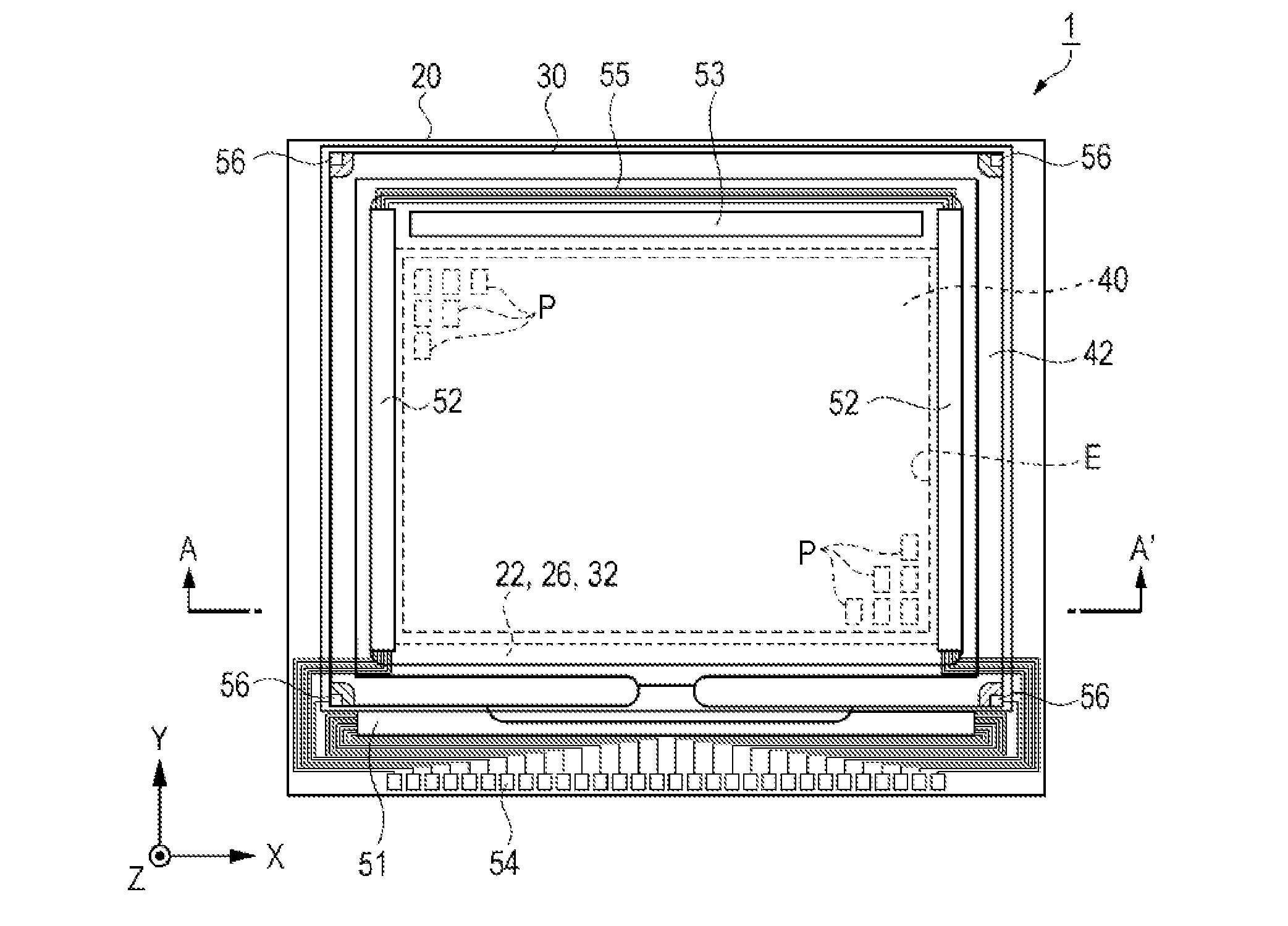
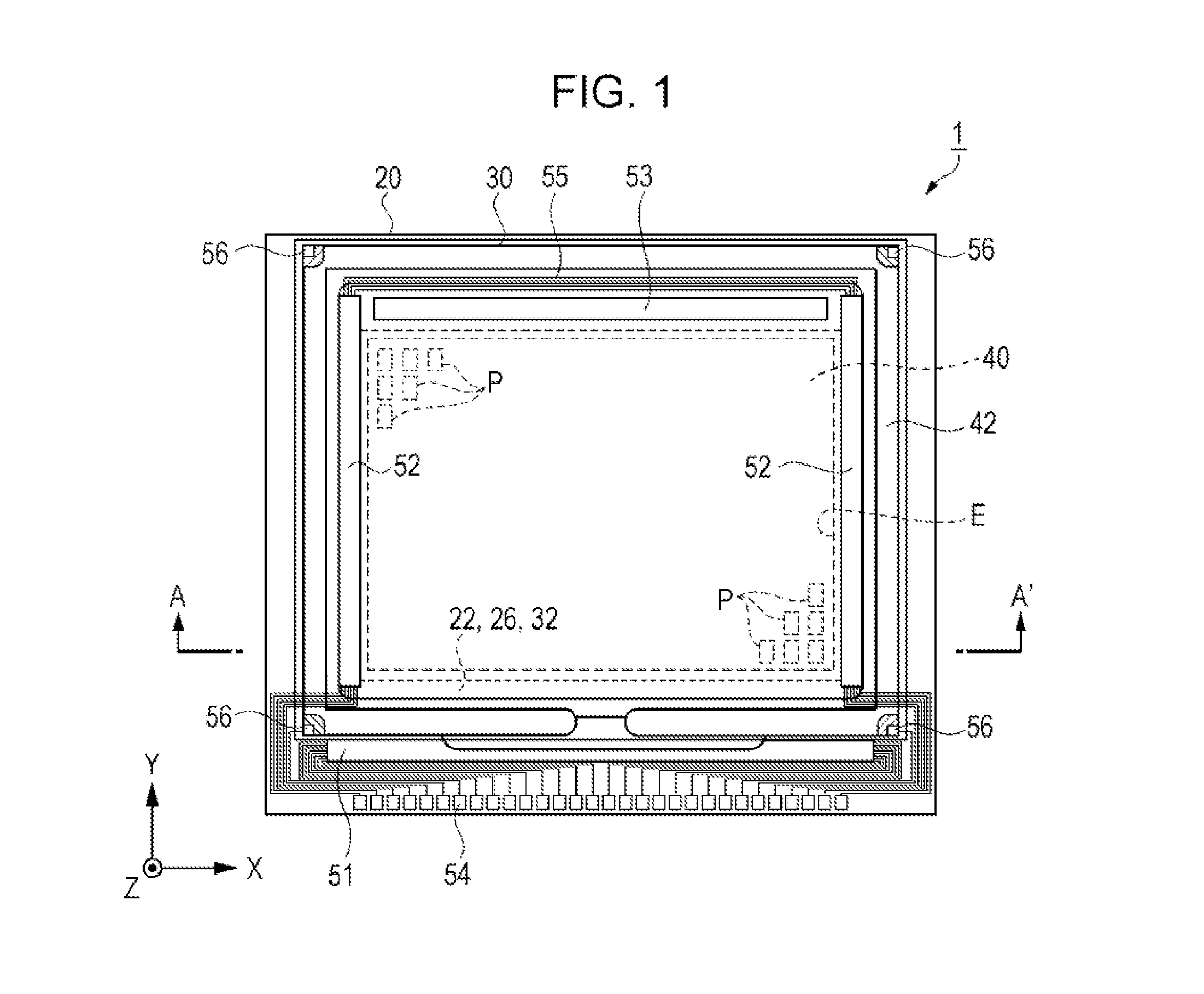
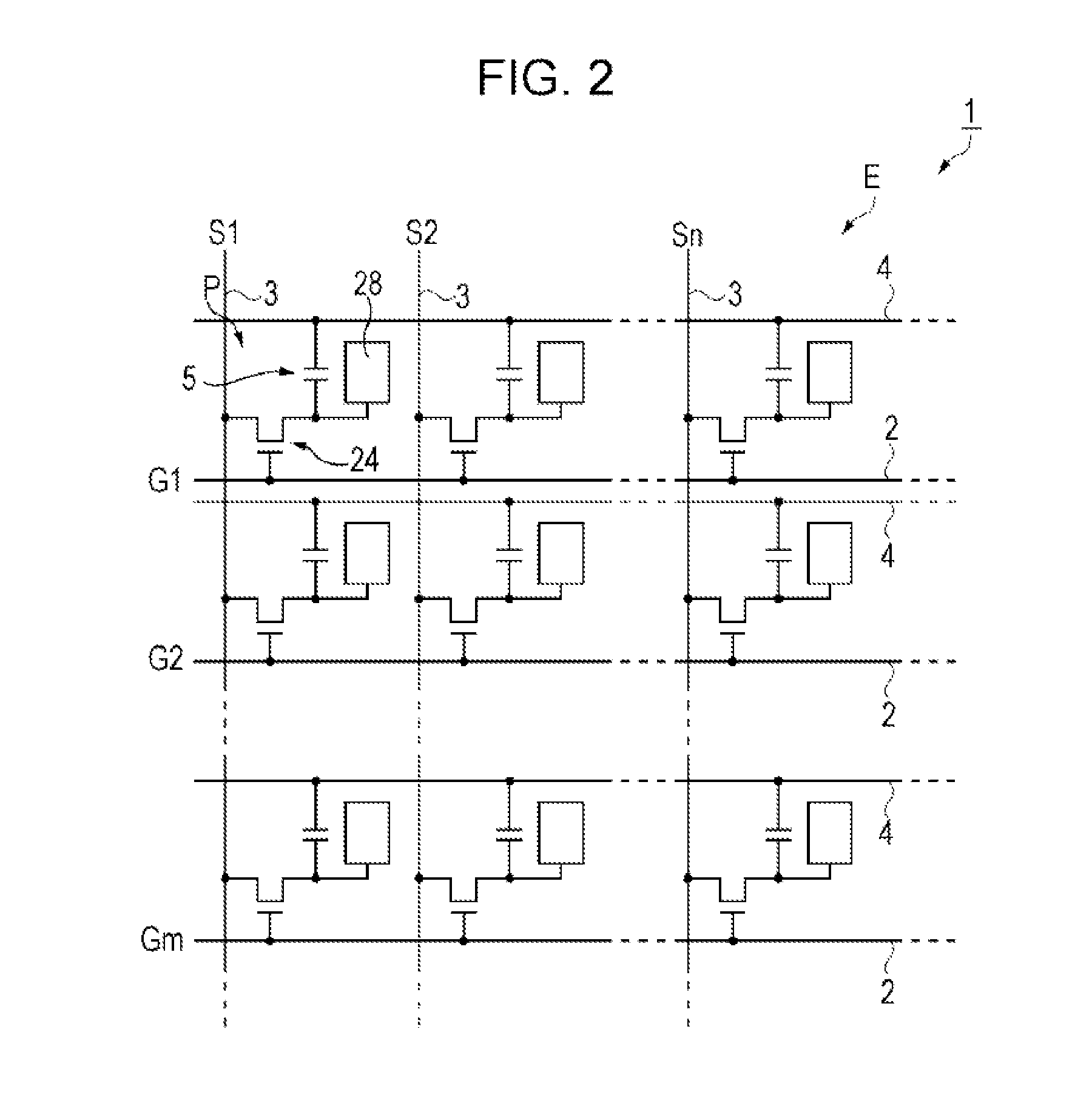
[0052]First, the liquid crystal device as the electro-optical device according to a first embodiment is described referring to FIG. 1, FIG. 2 and FIG. 3. FIG. 1 is a schematic plan view illustrating a configuration of the liquid crystal device according to the first embodiment. FIG. 2 is an equivalent circuit diagram illustrating an electric configuration of the liquid crystal device according to the first embodiment. FIG. 3 is a schematic cross-sectional view illustrating a configuration of the liquid crystal device according to the first embodiment. Specifically, FIG. 3 is a schematic cr...

second embodiment

[0114]Liquid crystal devices according to second and later embodiments are different in configuration of the micro lens array substrate, but because the other configurations are almost the same, a configuration of the micro lens array substrate and a method of manufacturing the micro lens array substrate are described, and descriptions of the other parts of the liquid crystal device are omitted.

Micro Lens Array Substrate

[0115]The configuration of the micro lens array substrate according to the second embodiment is described. FIG. 10 is a schematic plan view illustrating the configuration of the micro lens array substrate according to the second embodiment. FIGS. 11A and 11B are schematic cross-sectional views, each illustrating the configuration of the micro lens array substrate according to the second embodiment. Specifically, FIG. 11A is a schematic cross-sectional view taken along a line A-A′ (X-direction) in FIG. 10, and FIG. 11B is a schematic cross-sectional view taken along a...

third embodiment

Micro Lens Array Substrate

[0130]Next, a configuration of a micro lens array substrate according to a third embodiment is described. FIG. 12 is a schematic plan view illustrating the configuration of the micro lens array substrate according to the third embodiment. FIGS. 13A and 13B are schematic cross-sectional views, each illustrating the configurations of the micro lens array substrate according to the third embodiment. Specifically, FIG. 13A is a schematic cross-sectional view taken along a line A-A′ (X-direction) in FIG. 12, and FIG. 13B is a schematic cross-sectional view taken along a line B-B (W-direction) in FIG. 12.

[0131]A micro lens array substrate 10B according to the third embodiment is different from the micro lens array substrates 10 and 10A according to the embodiment described above in that a discontinuous part is provided along the thickness direction on a lens layer 12, but the micro array substrates 10, 10A, and 10B are almost the same in the other configurations....


PUM


Abstract

A micro lens array substrate includes a substrate having optical transparency and a lens layer having optical transparency and a different refractive index from that of the substrate, which is formed in such a manner as to fill in a concave portion arranged in one surface of the substrate in the X-direction, the Y-direction, and the W-direction. A through-hole is provided in the lens layer, between the adjacent concave portions in the W-direction in the lens layer, and the lens layer is continuous between the adjacent concave portions in the X-direction or in the Y-direction.

Description

BACKGROUND[0001]1. Technical Field[0002]The present invention relates to a micro lens array substrate, a method of manufacturing the micro lens array substrate, an electro-optical device and an electronic apparatus.[0003]2. Related Art[0004]An electro-optical device has been known that is equipped with an electro-optic material (for example, liquid crystal and the like) between an element substrate and an opposite substrate. A liquid crystal device used as a liquid crystal light valve of a projector can be among examples of the electro-optical device. An attempt has been made to realize high efficiency of utilization of light for such a liquid crystal device.[0005]Incidentally, for example, a configuration has been known in which at least one of the element substrate and the opposite substrate of the liquid crystal device includes the micro lens array substrate and thus light incident on the liquid crystal device is gathered. The configuration accomplishes a substantial improvement ...

Claims


Application Information

Patent Timeline
Patent Type & Authority Applications(United States)
IPC IPC(8): G02F1/1335
CPCG02F1/133526G02F1/133565G02F1/133607G02B3/0043G02B3/0056G02B27/149G02F1/133512G02F1/136286G02F1/1368G02F2201/123G03B21/006G03B33/12
Inventor NIMURA, TORU
Owner SEIKO EPSON CORP
Why Eureka
Try Eureka