Light-emitting diode and method for preparing the same

Active Publication Date: 2014-05-29
HC SEMITEK CORP
View PDF7 Cites 8 Cited by
  • Summary
  • Abstract
  • Description
  • Claims
  • Application Information

AI Technical Summary

Benefits of technology

[0021]The method of the invention stripping the sapphire substrate by a wet process rather than the laser or the mechanical grinding method causes low damage to the epitaxial layer and can strip the sapphire substrate completely. The performance of the light-emitting diode havin

Problems solved by technology

The luminous efficiency of the GaN base light-emitting diode is significantly improved in recently years, but it cannot completely replace the conventional light resource.
At present, the quantum efficiency, the current distribution uniformity and device cooling capacity has become main technical bottlenecks which limit further improvements of the performance of light-emitting diodes.
The main disadvantages of the semiconductor light-emitting diodes with lateral structure include low heat dissipation efficiency, current congestion, low current density and high production cost.
However, the flip chip technology is very complicated and the production cost is high.
In addition, the sapphire which is usually used as a support substrate of a light-emitting diode has drawbacks that the electrical conductivity is very low and its lattice constant does not match with the GaN material.
The thermal resistant of the device is increased due to the very low electrical conductiv

Method used


Image

  • Light-emitting diode and method for preparing the same
  • Light-emitting diode and method for preparing the same
  • Light-emitting diode and method for preparing the same

Examples


example 1

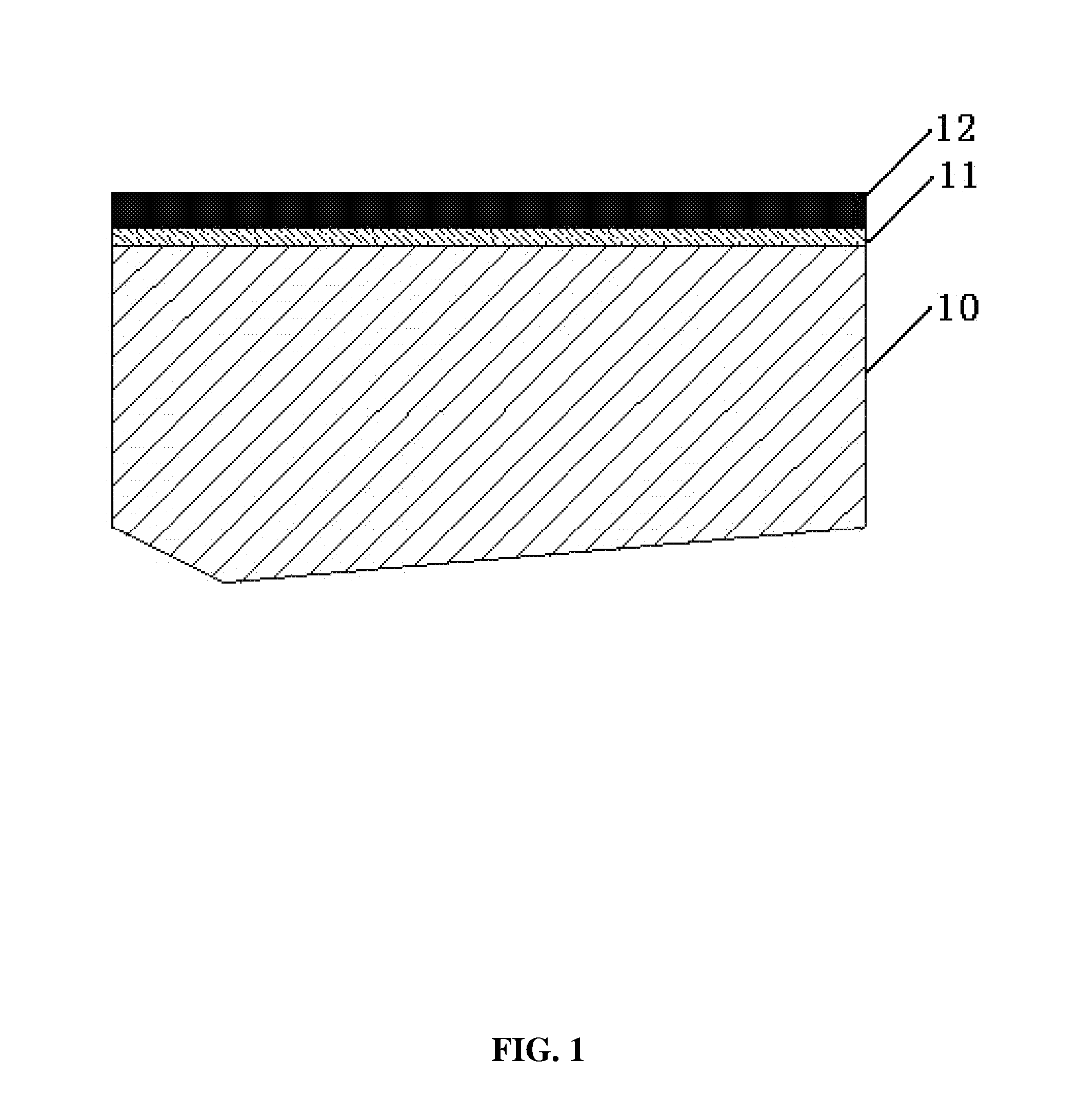
[0132]As shown in FIG. 1, a SiO2 film of 7000 angstrom and a SiNx film 12 of 8000 angstrom are respectively deposited on a sapphire substrate 10 by chemical vapor deposition.

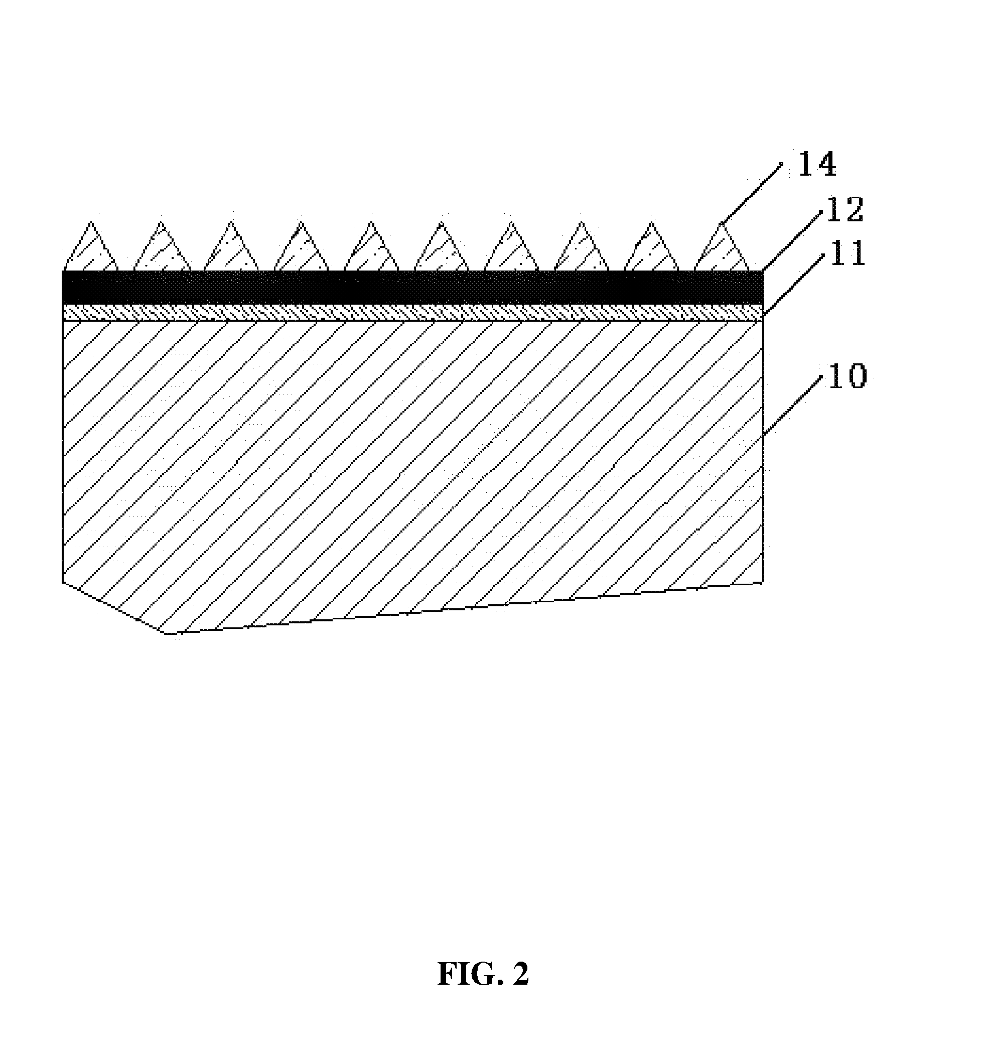
[0133]As shown in FIG. 2, a stripe mask pattern is prepared in the SiNx film using photoresists. The section of a stripe pattern is approximately triangle, and the bottom width of the section is 2.4 micron, the height of the section is 2 micron, the distance between two adjacent stripe patterns is 0.6 micron. The vertical view is illustrated in FIG. 3.

[0134]As shown in FIG. 4, the pattern of the photoresists is transferred to the SiNx film and the SiO2 film to form a graphical substrate by dry etching. The section of the stripe pattern is approximately triangle, and the bottom width of the section is 2.5 micron, the height of the section is 1.5 micron. A thickness of the SiO2 film is 0.7 micron, and a thickness of the SiNx film is 0.8 micron.

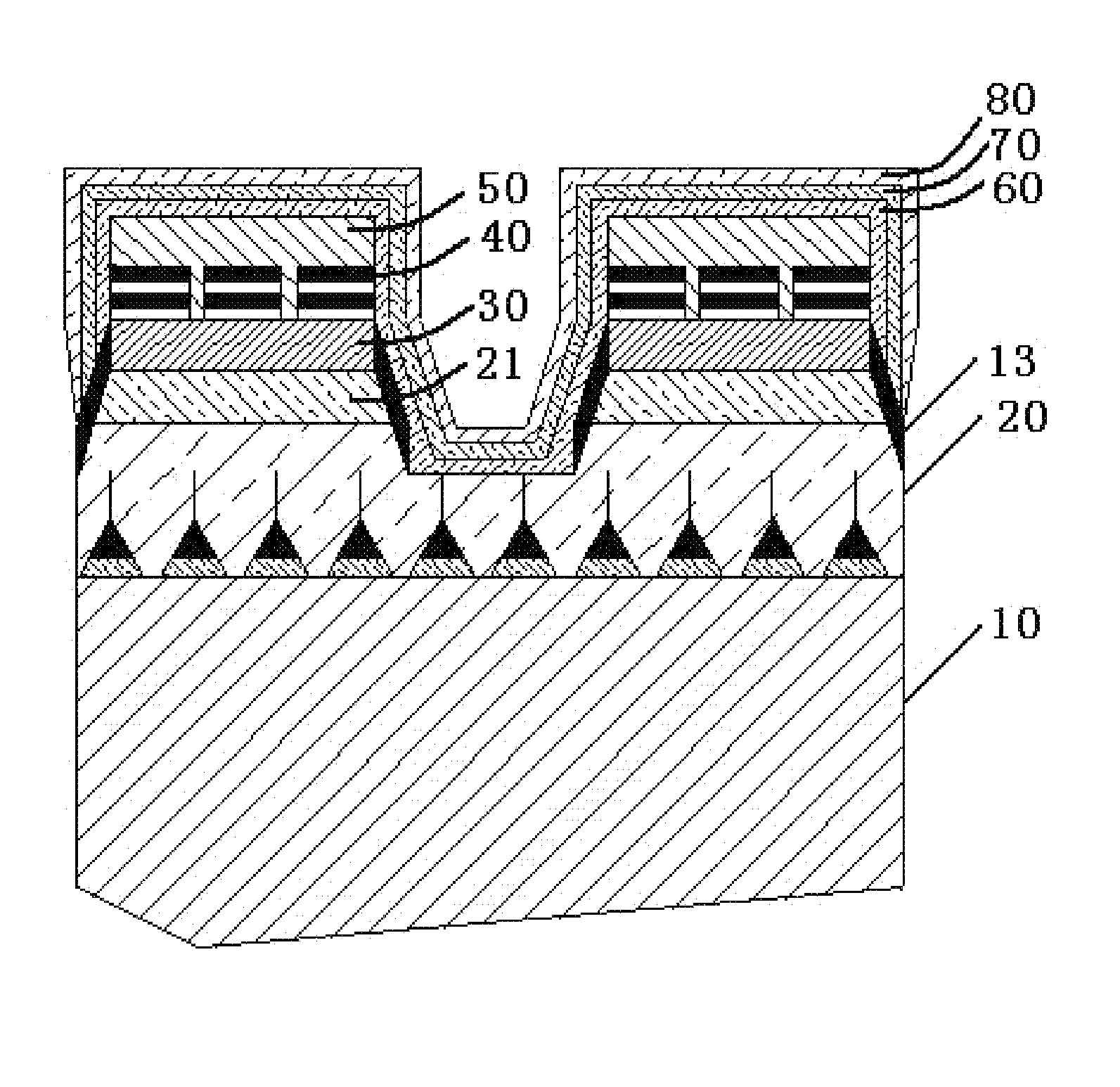
[0135]As shown in FIG. 5, growing a GaN base light-emitting diode epita...

example 2

[0154]As shown in FIG. 24, a SiO2 film 11 of 10000 angstrom and a SiNx film 12 of 8000 angstrom are respectively deposited on a sapphire substrate 10.

[0155]As shown in FIG. 25, a mesh mask pattern is prepared in the SiNx film using photoresists. The section of the mask is approximately triangle, and the bottom width of the section is 2.4 micron, the height of the section is 2.5 micron, the distance between two adjacent stripe patterns is 0.8 micron. The vertical view is illustrated in FIG. 26.

[0156]As shown in FIG. 27, the pattern of the photoresists is transferred to the SiO2 film and the SiNx film by dry etching to form a mesh pattern. The section of the pattern is approximately triangle, and the bottom width of the section is 2.4 micron, the height of the section is 1.8 micron. A thickness of the SiO2 film is 1.0 micron, and a thickness of the SiNx film is 0.8 micron.

[0157]As shown in FIG. 28, growing a GaN base light-emitting diode epitaxial layer including a N-type layer 20 and...


PUM


Abstract

A method for preparing a light-emitting diode having a vertical structure by stripping a GaN base epitaxial layer and a sapphire substrate by a wet process, the method including: a) preparing a graphical growth substrate; b) growing a GaN base light-emitting diode epitaxial layer on the graphical growth substrate, the GaN base light-emitting diode epitaxial layer from the bottom to the top successively including a N-type GaN layer and a P-type GaN layer; c) successively forming a transparent and electrically conductive film, an omni-directional reflection layer, an electrically conductive reflection layer, and a passive metal protection layer from the bottom to the top on the GaN base light-emitting diode epitaxial layer; and d) removing the first layer of stable material with a high melting point of the growth substrate by dry etching, exposing the N-type GaN layer, and preparing an N electrode on the N-type GaN layer.

Description

CROSS-REFERENCE TO RELATED APPLICATIONS[0001]This application is a continuation-in-part of International Patent Application No. PCT / CN2012 / 079246 with an international filing date of Jul. 27, 2012, designating the United States, now pending, and further claims priority benefits to Chinese Patent Application No. 201110217923.9 filed Aug. 1, 2011. The contents of all of the aforementioned applications, including any intervening amendments thereto, are incorporated herein by reference. Inquiries from the public to applicants or assignees concerning this document or the related applications should be directed to: Matthias Scholl P.C., Attn.: Dr. Matthias Scholl Esq., 14781 Memorial Drive, Suite 1319, Houston, Tex. 77079.BACKGROUND OF THE INVENTION[0002]1. Field of the Invention[0003]The present invention relates to a method for preparing a light-emitting diode having a vertical structure, and more particularly to a method for preparing a light-emitting diode having a vertical structure ...

Claims


Application Information

Patent Timeline
IPC IPC(8): H01L33/00H01L33/60
CPCH01L33/20H01L2933/0091H01L33/007H01L33/46H01L21/0242H01L21/0254H01L21/02639H01L21/02647H01L33/0093H01L2924/12041H01L33/0075H01L33/60
Inventor XU, JINWANG, JIANGBOLIU, RONG
Owner HC SEMITEK CORP
Why Eureka
Try Eureka