Cmp pad conditioner

a technology of mechanical polishing and conditioner, which is applied in the direction of grinding drive, grinding drive, abrasive surface conditioning device, etc., can solve the problems of non-uniform deformation of the surface of the polishing pad, limitation that cannot be overcome by partial planarization, and the minimum line width can be reduced, so as to achieve efficient removal of debris, increase the productivity of the cmp pad conditioner, and fast and easy manner

Active Publication Date: 2014-06-05
NIWA DAIYAMONDO INDS
View PDF5 Cites 10 Cited by
  • Summary
  • Abstract
  • Description
  • Claims
  • Application Information

AI Technical Summary

Benefits of technology

[0041]The present invention has the following excellent effects.
[0042]First, in the CMP pad conditioner of the present invention, the cutting tip patterns can be formed in a fast and easy manner so that the productivity of the CMP pad conditioner can be increased.
[0043]Also, in the CMP pad conditioner of the present invention, the cutting tip patterns formed may have a fine structures wherein the strength and stability thereof are ensured.
[0044]Lastly, in the CMP pad conditioner of the present invention, the cutting tip patterns efficiently remove debris and expel foreign matter, such as sludge, during a conditioning process.

Problems solved by technology

However, with an increase in the integration density of devices and a decrease in the minimum line width, limitations that cannot be overcome by partial planarization, according to the related art, have arisen.
However, because different pressures and relative speeds are applied during the polishing process, the surface of the polishing pad can become non-uniformly deformed with the passage of time during the polishing, and the pores on the polishing pad can become clogged with the polishing residue, wherein the polishing pad cannot perform its intended function.
For this reason, uniform polishing of the wafer surface by global planarization cannot be accomplished.
However, these conventional electrodeposited-type and melted-type CMP pad conditioners have a problem in that, when they are used for in-situ conditioning in the metal CMP process, diamond particles attached to the surface of the CMP pad conditioners become detached from the surface via the action of polishing via the polishing particles of the CMP slurry and surface corrosion caused by the acidic solution.
When the detached diamond particles are stuck in the CMP polishing pad during the CMP polishing process, they scratch the water surface to increase process defect rates and make it necessary to replace the CMP polishing pad.
In addition, metal ions released from the metal binder via corrosion move to the metal line of a semiconductor circuit during the metal CMP process and can cause metal ion contamination, which causes short circuits.
Because the short circuits caused by metal ion contamination are only revealed after all of the processes have been completed, the loss of production cost via the metal ion contamination is significant.
These tips can produce minor cuts on a polyurethane polishing pad during a conditioning process, but cannot finely crush large debris generated during the conditioning process, nor efficiently sweep out the sludge that is generated from the wafer.
However, this CMP pad conditioner has the following two problems.
Another problem is that diamonds have extremely low impact strength due to their high brittleness, even though diamonds have high hardness.
Considering conditioner pressure and abrasion via friction with the polishing material, which occur via finely cutting the tip patterns during polishing of the polishing pad in the CMP system, the stability of the cutting patterns against breakage and detachment cannot be ensured.
This breakage and detachment of the cutting tip patterns cause scratches to form on the silicon wafers.
However, it is difficult to form fine cutting tip patterns having a size of 100 μm because CVD diamond layers grow into columnar structures that are very weak against the shear loads applied during the conditioning process.

Method used


Image

  • Cmp pad conditioner
  • Cmp pad conditioner
  • Cmp pad conditioner

Examples


Embodiment Construction

[0052]Hereinafter, the present invention will be described in detail with reference to the accompanying drawings.

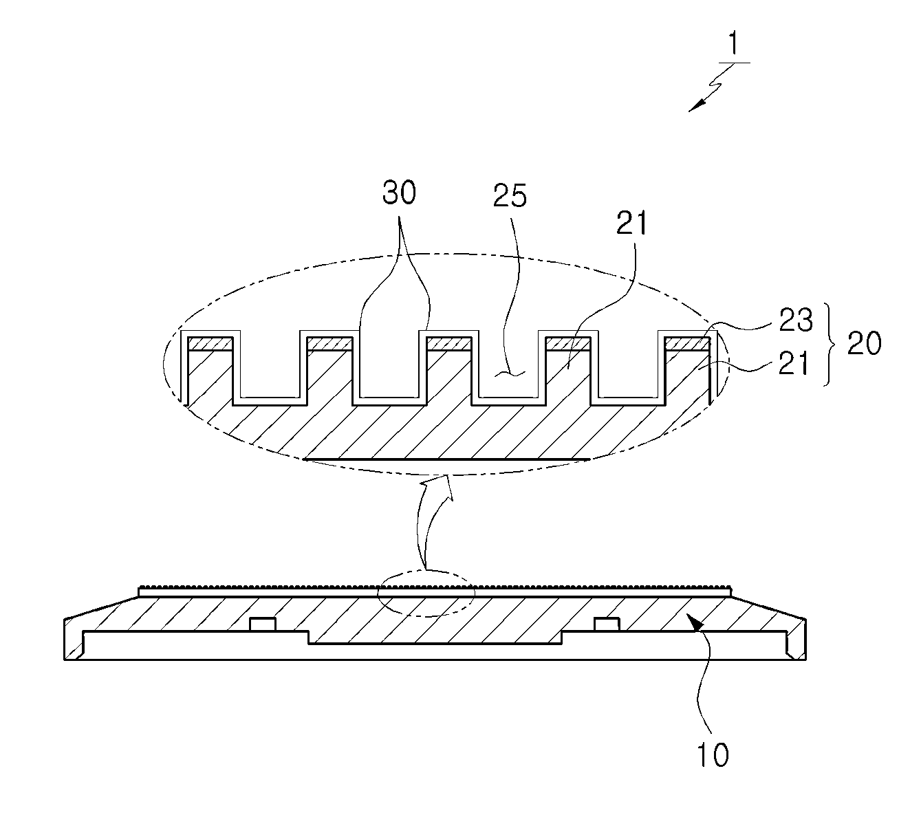
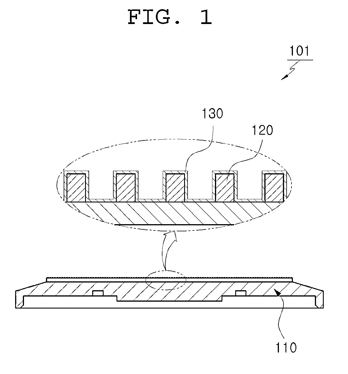
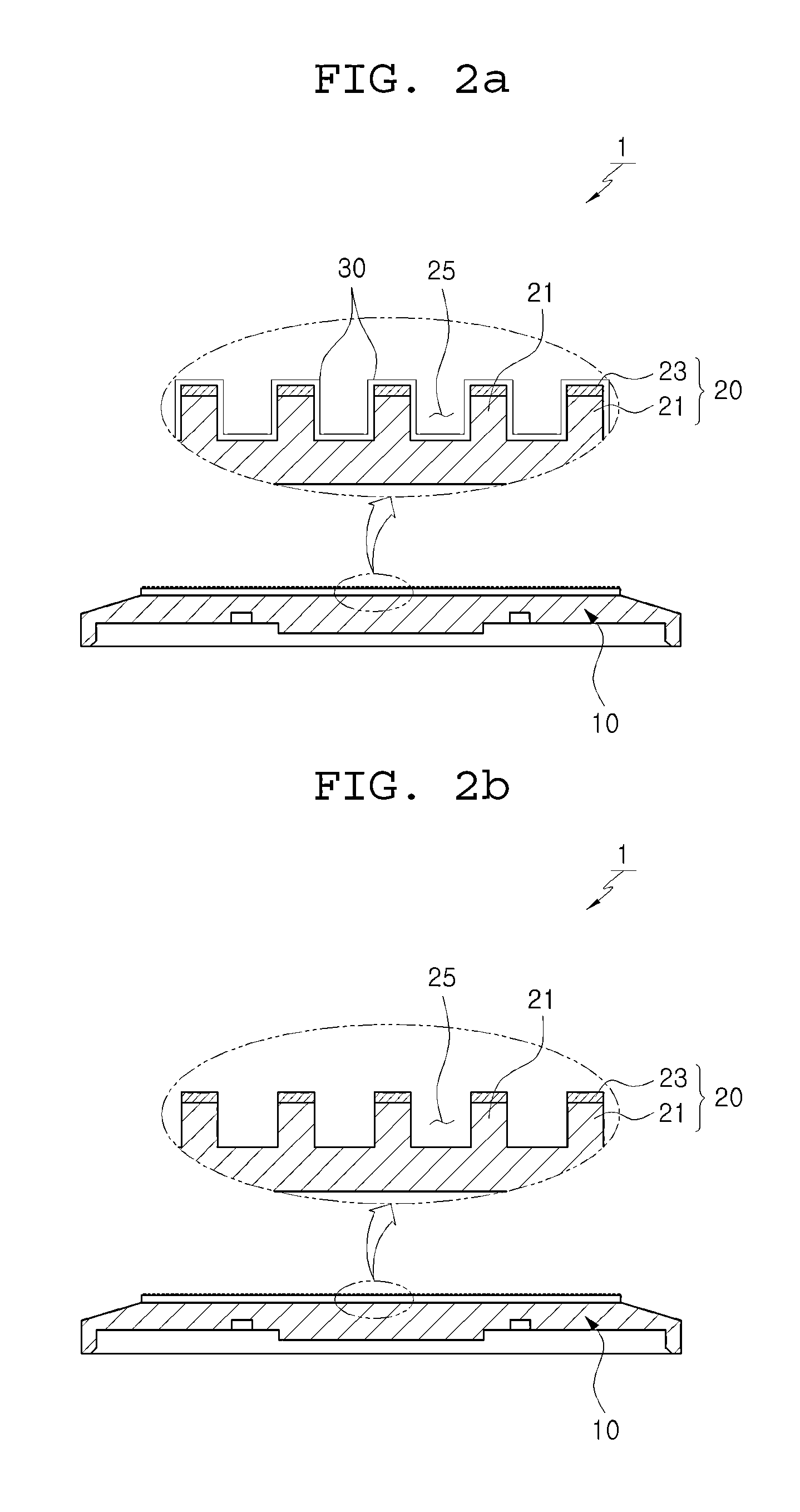
[0053]FIGS. 2a, 2b, 3a, and 3b are cross-sectional views of CMP pad conditioners wherein all the cutting tips of cutting patterns include substrate tip portions and deposition tip portions. FIGS. 4a, 4b, 5a, and 5b are cross-sectional views of CMP pad conditioners wherein only some of the cutting tips of cutting patterns include substrate tip portions and diamond deposition tip portions. As shown in these figures, a CMP pad conditioner 1, according to the present invention, includes a substrate 10 and cutting tip patterns 20 formed on at least one surface of the substrate 10.

[0054]The substrate 10 may be made of a high-hardness material, such as a general iron alloy, a super-hard alloy, or a ceramic material, and may have a disc shape.

[0055]Herein, the material of the substrate 10 is preferably at least one selected from among SiC, silicon nitride (Si3N4), tungsten carbid...


PUM


Abstract

The present invention relates to a CMP pad conditioner having a substrate and a cutting tip pattern formed on at least one surface of the substrate, and more particularly to a CMP pad conditioner having cutting tip patterns, in which the cutting tip patterns have an improved structure that can increase the productivity of the CMP pad conditioner and that can sufficiently ensure the strength and safety of the cutting tip patterns.

Description

CROSS REFERENCE TO RELATED APPLICATIONS AND CLAIM OF PRIORITY[0001]This patent application is a National Phase application under 35 U.S.C. §371 of International Application No. PCT / KR2012 / 005649, filed 16 Jul. 2012, which claims priority to Korean Patent Application numbers 10-2011-0070924, filed 18 Jul. 2011, and 10-2012-0066596, filed 21 Jun. 2012, entire contents of which are incorporated herein by reference.BACKGROUND[0002]1. Field of the Invention[0003]The present invention relates to a chemical mechanical polishing (CMP) pad conditioner having a substrate and a cutting tip pattern formed on at least one surface of the substrate.[0004]2. Description of the Related Art[0005]Currently, the speed and integration density of semiconductor circuits are increasing, and thus the size of semiconductor chips is gradually increasing. In addition, in order to provide multilayer interconnection structures, the width of interconnections is being minimized and the diameter of the wafers is be...

Claims


Application Information

Patent Timeline
Patent Type & Authority Applications(United States)
IPC IPC(8): B24B53/017
CPCB24B53/017B24B53/12H01L21/304
Inventor LEE, SEH KWANGLEE, JOO HAN
Owner NIWA DAIYAMONDO INDS
Why Eureka
Try Eureka