Integrated circuit common-mode filters with ESD protection and manufacturing method

a common-mode filter and integrated circuit technology, applied in the field of electromagnetic interference filters, can solve the problems of performance degradation of high-speed electronics, large and thick footprint, and is not suitable for advanced electronic devices, and achieve the effect of enhancing the inductive coupling

Active Publication Date: 2014-07-17
NANJING SILERGY SEMICON TECH CO LTD
View PDF9 Cites 16 Cited by
  • Summary
  • Abstract
  • Description
  • Claims
  • Application Information

AI Technical Summary

Benefits of technology

[0015]In one embodiment, the primary and secondary spiral coupled inductor coils of the CMF filter

Problems solved by technology

DVI, MIPI, etc.), which affects the useful signals and results in performance degradation of high-speed electronics.
These common-mode choke coils are essentially discrete CMF components fabricated using various discrete component processing techniques, which translates into relatively large and thick footprint, hence making them not suitable for advanced electronic apparatus, such as smart-phones, which require very thin and small CMF components w

Method used


Image

  • Integrated circuit common-mode filters with ESD protection and manufacturing method
  • Integrated circuit common-mode filters with ESD protection and manufacturing method
  • Integrated circuit common-mode filters with ESD protection and manufacturing method

Examples


first embodiment

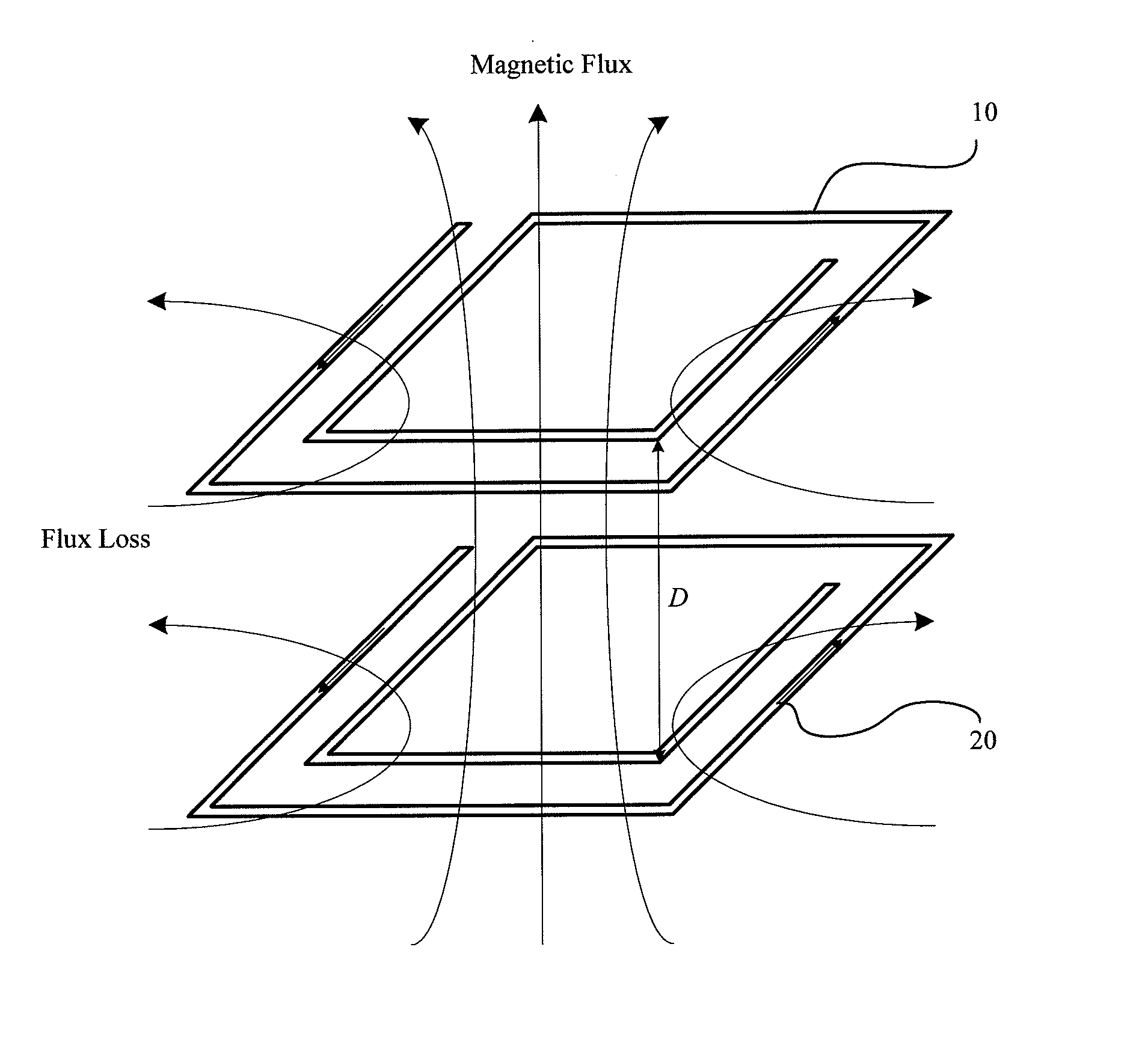
[0049]For an ideally coupled CMF structure, we have k=1, which means no loss of magnetic flux between the two spirals. Unlike in discrete ferrite or ceramics based CMF structures where magnetic cores serve to enhance magnetic coupling, it is generally difficult to integrate magnetic materials into IC processes. Hence, the CMF structure in the first embodiment does not have any magnetic medium integrated. As illustrated in FIG. 7, to achieve good magnetic coupling inside an IC CMF structure (i.e., a higher k), careful layout design is required to ensure exact same spiral layout shape for the two inductor coils, which should be overlapping each other closely. In addition, a vertical distance (D) between the two inductor spirals in the thickness direction should be as short as possible to ensure excellent magnetic coupling, hence the highest possible k value. However, a smaller D directly results in a larger coupling capacitance Ci, which dramatically degrades the signal integrity of t...

third embodiment

[0052]Moreover, please refer to FIG. 9A and FIG. 9B for the second and third embodiment of the present invention, wherein FIG. 9A shows an embodiment of the CMF filter including the primary spiral inductor coil and the secondary spiral inductor coil having the same layout shapes and completely overlapping each other vertically. FIG. 9B shows an embodiment of the CMF filter including the primary spiral inductor coil and the secondary spiral inductor coil having the same layout shapes, but do not overlap each other completely.

[0053]As shown in the embodiments of FIG. 9A, since the primary spiral inductor coil 10 and the secondary spiral inductor coil 20 have the same layout shapes and completely overlap each other vertically, the CMF filter achieves the highest coupling effect of k≧0.97. However, the coupling capacitance Ci becomes very large, which results in severe degradation of differential mode signals and very low fC. Another major problem associated to the complete-overlap layo...

fourth embodiment

[0055]Refer to FIG. 11 for the present invention, in which FIG. 11 shows a layout illustration of an exemplar 4-metal-layer CMF filter circuit structure in accordance with one embodiment of the present invention. In this embodiment, the primary spiral inductor coil is implemented by using multiple metal layers, i.e., the metal layers 1 and 3 (from the bottom), while the secondary spiral inductor coil is implemented by using the metal layer 2 and 4.

[0056]In the fourth embodiment, multiple-layer metal spirals (i.e., stacked spirals 1-4), separated by dielectric layers, are used to form both primary and secondary inductor coils that occupy alternative layers.

[0057]The multiple-layer stacked spiral structures not only deliver the required very high inductance values (typically more than 100 nH), but also significantly enhances the inductive coupling effect between the primary and secondary coils due to its inter-digitized layer structure. Therefore, the multiple-layer CMF filter as show...


PUM


Abstract

An integrated circuit common-mode electromagnetic interference filter incorporating electro-static discharge protection comprising two inductive coils is provided. A pair of primary and secondary spiral inductor coils is disposed corresponding to each other. A dielectric layer is used to separate the primary spiral inductor coil from the secondary spiral inductor coil electrically. Resistivity of a high-resistance substrate is more than 100 Ω-cm for supporting the primary spiral inductor coil, the secondary spiral inductor coil and the dielectric layer thereon. The proposed filter structure can be formed in integrated circuit (IC) back-end processes and thus be extraordinarily advantageous of effectively eliminating electromagnetic interferences and having electrostatic protection effect at the same time, while having small footprint.

Description

BACKGROUND OF THE INVENTION[0001]1. Field of the Invention[0002]The present invention relates to electromagnetic interference (EMI) filters in integrated circuit (IC) format incorporating electro-static discharge (ESD) protection components, and the manufacturing method[0003]2. Description of the Prior Art[0004]Electromagnetic interference (EMI) can affect electronic system performance, especially at electronic interfaces, e.g., Mobile Industry Processor Interface (MIPI), Universal Serial Bus (USB), High Definition Multimedia Interface (HDMI) and Mobile High-Definition Link (MHL), etc., which feature very high data transmission rates and very broad frequency bandwidth. Low-pass filters (LPF) can be used to block EMI interferers (or, noises) transmitting in both directions at the interfaces of electronic products. Critical specifications (i.e., specs) for EMI filters include low pass-band insertion loss (IL), high cut-off frequency (fC), wide pass-band spectrum and high rejection-ban...

Claims


Application Information

Patent Timeline
IPC IPC(8): H02H9/04
CPCH02H9/044H01L23/5227H01F17/0013H01L27/0288H01L28/10H01L2924/0002H03H7/427
Inventor WANG, ALBERT Z.WU, WEN-CHINWANG, SHIJUNZHANG, NAN
Owner NANJING SILERGY SEMICON TECH CO LTD
Why Eureka
Try Eureka