Semiconductor device and method of manufacturing semiconductor device

a semiconductor and semiconductor technology, applied in the direction of individual semiconductor device testing, semiconductor/solid-state device testing/measurement, instruments, etc., can solve the problems of difficult heat treatment of activating the fs layer, low yield, and high risk of wafer breakage, so as to suppress an increase in leakage current and suppress the effect of on-voltag

Active Publication Date: 2014-08-07
FUJI ELECTRIC CO LTD
View PDF2 Cites 26 Cited by
  • Summary
  • Abstract
  • Description
  • Claims
  • Application Information

AI Technical Summary

Benefits of technology

[0048]According to the semiconductor device and the method of manufacturing the semiconductor device for embodiments of the invention, it is possible to suppress an increase in the on-voltage. In addition, according to the semiconductor device and the method of manufacturing the semiconductor de...

Problems solved by technology

However, in this method, it is difficult to perform heat treatment for activating the FS layer after the ions are implanted into the rear surface of the wafer at a temperature equal to or hig...

Method used


Image

  • Semiconductor device and method of manufacturing semiconductor device
  • Semiconductor device and method of manufacturing semiconductor device
  • Semiconductor device and method of manufacturing semiconductor device

Examples


embodiment 1

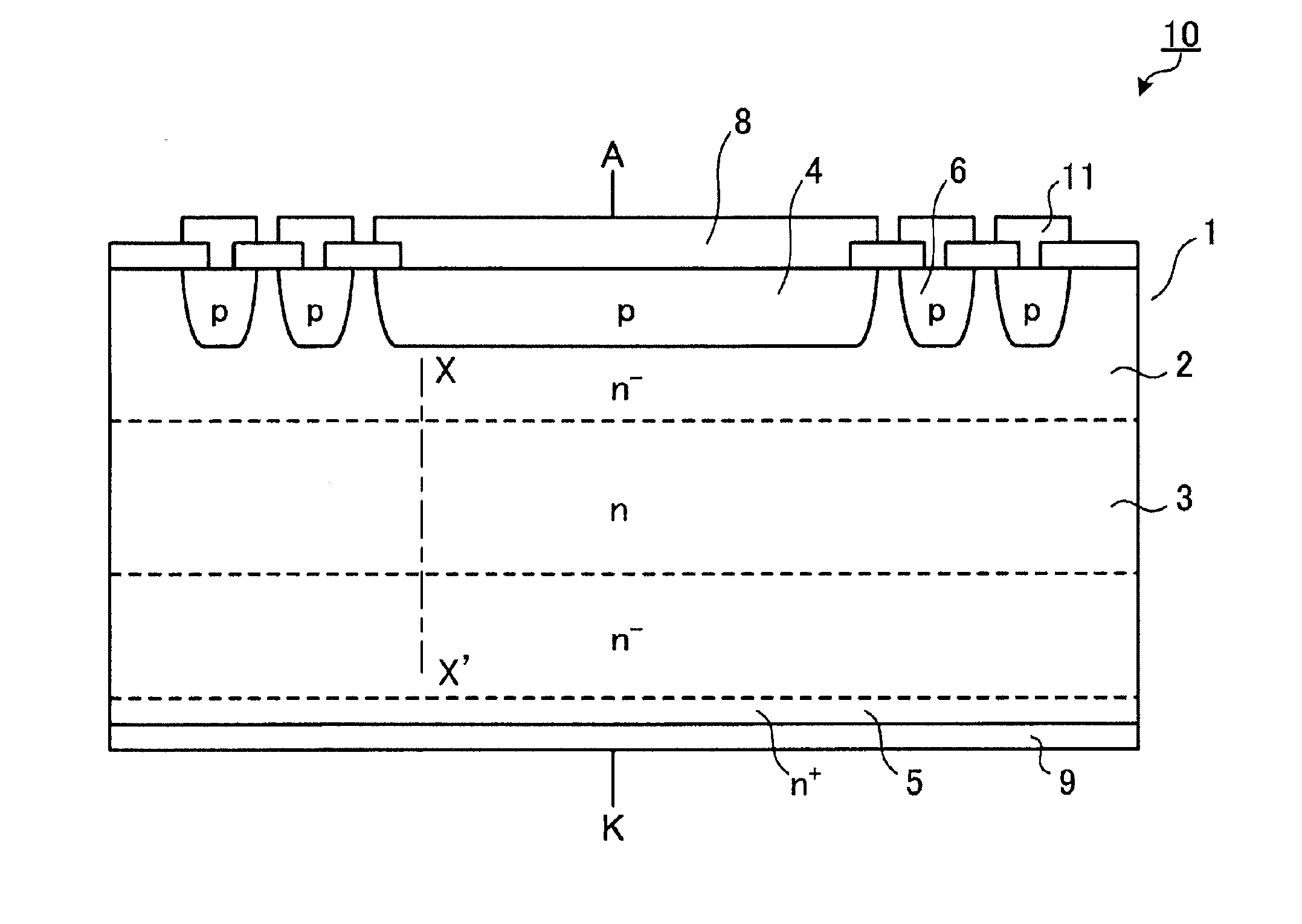
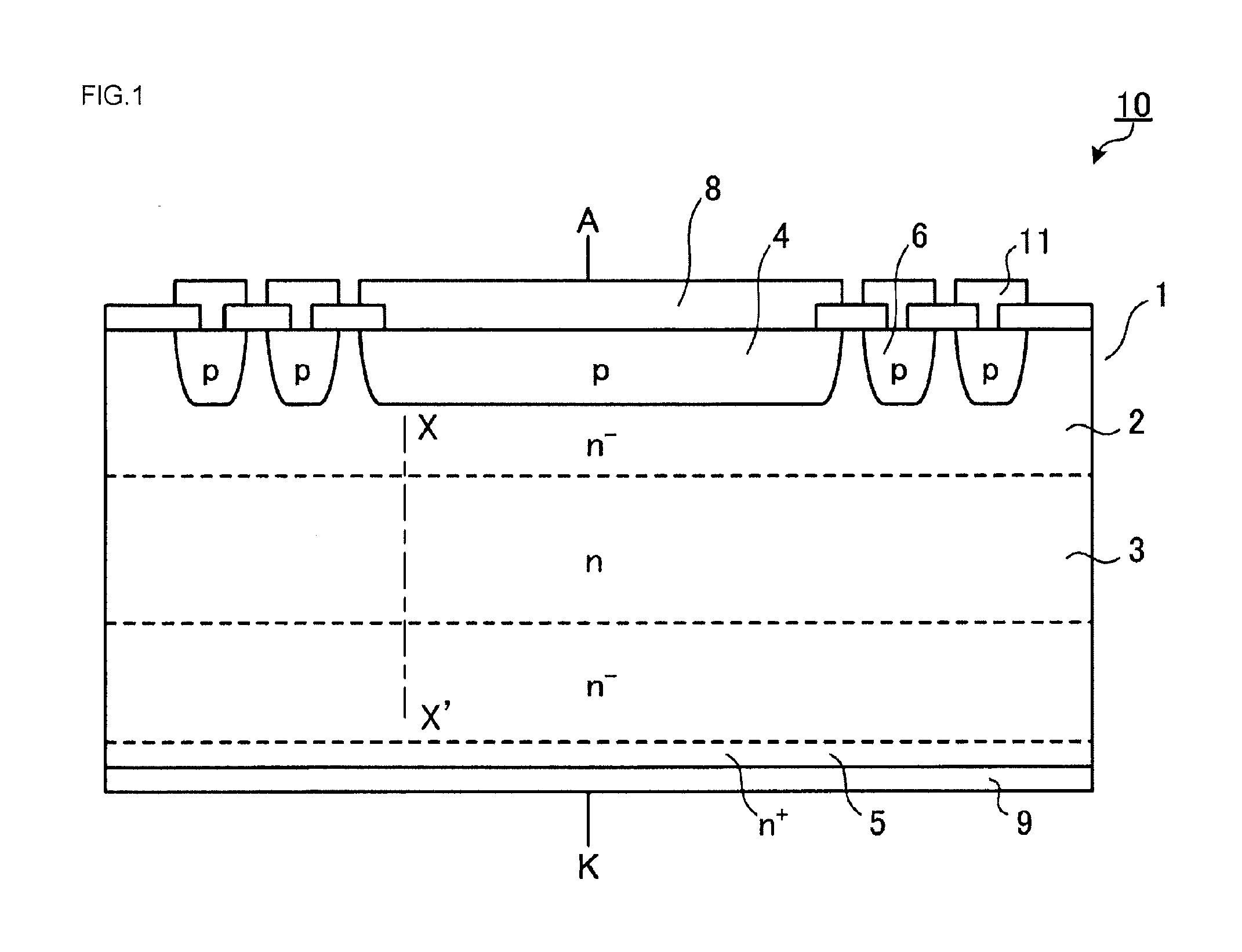
[0077]The structure of a semiconductor device according to embodiments of the invention will be described. FIG. 1 is a schematic cross-sectional view illustrating the structure of the semiconductor device according to the embodiments of the invention. The semiconductor device shown in FIG. 1 is a pin diode 10 including a BB layer which is a donor layer 3 formed by proton radiation. Specifically, the donor layer 3 is provided at a depth corresponding to near the center of an n-type drift layer 2 which is a silicon semiconductor substrate (n− semiconductor substrate) 1. When the donor layer 3 is formed, first, a crystal defect is formed in the n-type drift layer 2, which is the silicon semiconductor substrate 1, by proton radiation. In Example 1 which will be described below, a proton dose was 1×10¹² (atoms / cm2) and acceleration energy was 8 MeV (hereinafter, referred to as proton radiation conditions of this embodiment). After the proton radiation, a heat treatment is performed to ch...

embodiment 2

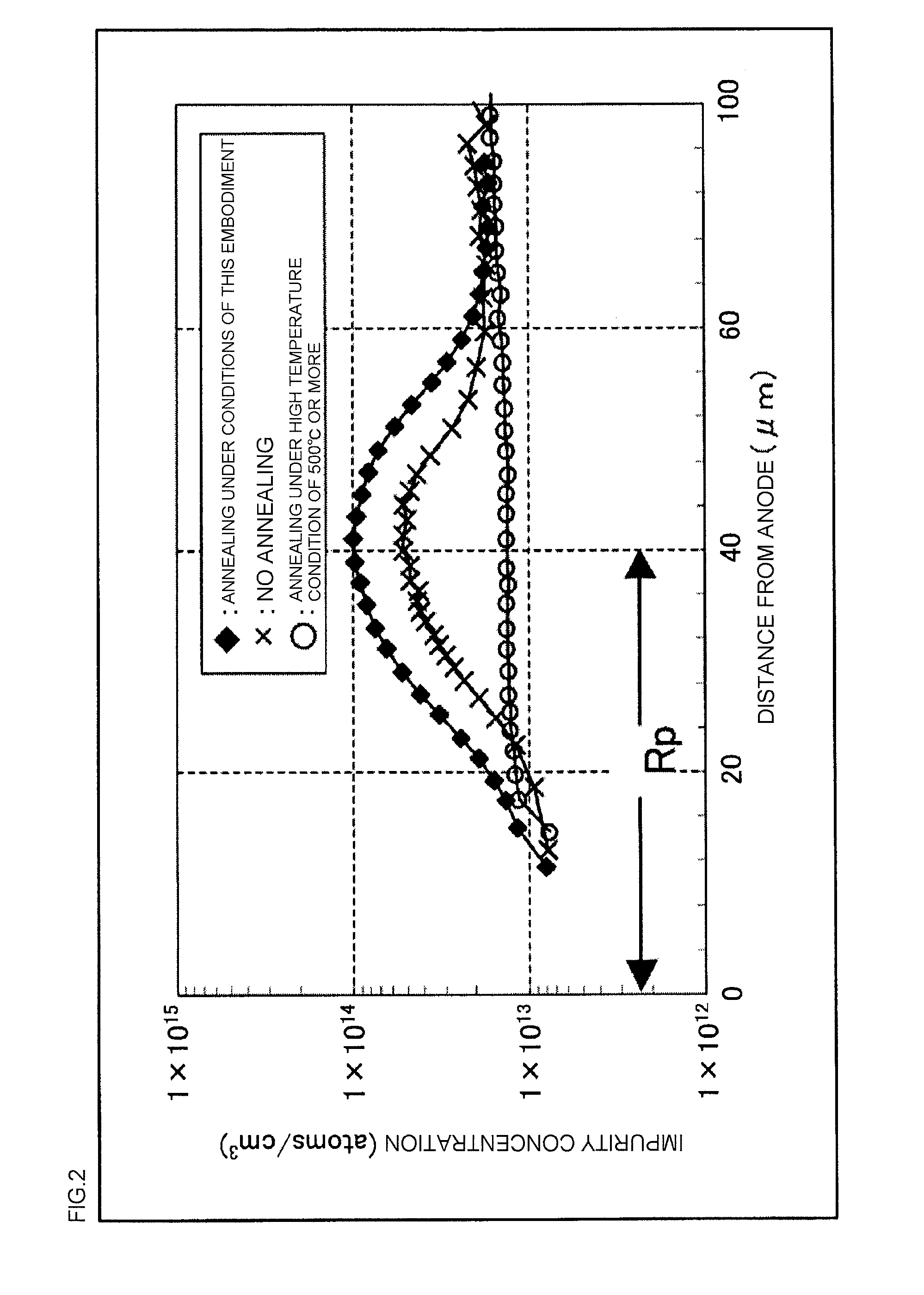
[0083]Next, the relationship between the peak intensity of a DLTS signal and an annealing temperature and the relationship between donor peak concentration and the annealing temperature when annealing is performed under the conditions of this embodiment, when no annealing is performed, and when annealing is performed under a high temperature condition of 500° C. or more. FIG. 3 is a characteristic diagram illustrating a DLTS spectrum waveform of a semiconductor device according to Example 1 after proton radiation. FIG. 4 is a characteristic diagram illustrating the relationship between the annealing temperature and the peak intensity of the DLTS signal after proton radiation in the semiconductor device according to Example 1. FIG. 5 is a characteristic diagram illustrating the relationship between the annealing temperature and the donor peak concentration after proton radiation in the semiconductor device according to Example 1.

[0084]FIG. 3 shows the spectrum waveform which is the D...

embodiment 3

[0098]Next, a method of manufacturing the semiconductor device according to embodiments of the invention will be described in detail. In this embodiment, an example in which the pin diode with a breakdown voltage of 1200 V shown in FIG. 1 is manufactured will be described. An FZ-n-type silicon semiconductor substrate 1 (hereinafter, referred to as a wafer 1) with a resistivity of 90 Ωcm (a phosphorus concentration of 5.0×10¹³ atoms / cm3) is prepared as the silicon semiconductor substrate. A heat treatment is performed in a nitrogen and oxygen atmosphere at a temperature of 1250° C. for 100 hours to thermally diffuse phosphorus to a depth of about 80 μm from both main surfaces of the wafer 1. The surface impurity concentration of a phosphorus diffusion layer formed in the wafer 1 is, for example, about 1.0×10²⁰ atoms / cm3. A large amount of oxygen is introduced from both surfaces of the wafer 1 into the wafer 1 by the heat treatment and the oxygen concentration of the wafer 1 becomes s...


PUM


Abstract

A donor layer that is formed by performing a heat treatment for a crystal defect formed by proton radiation is provided in an n-type drift layer of an n semiconductor substrate. The donor layer has an impurity concentration distribution including a portion with the maximum impurity concentration and a portion with a concentration gradient in which the impurity concentration is reduce to the same impurity concentration as that of the n-type drift layer in a direction from the portion with the maximum impurity concentration to both surfaces of the n-type drift layer. The crystal defect formed in the n-type drift layer is a composite crystal defect mainly caused by a vacancy, oxygen, and hydrogen.

Description

CROSS-REFERENCE TO RELATED APPLICATIONS[0001]This application is a continuation application, filed under 35 U.S.C.§111(a), of International Application PCT / JP2012 / 079674 filed on Nov. 15, 2012, and claims foreign priority benefit of Japanese Patent Application 2011-249982 filed on Nov. 15, 2011 in the Japanese Patent Office, the disclosures of both of which are incorporated herein by reference.BACKGROUND[0002]1. Field[0003]Embodiments of the invention relate to a semiconductor device and a method of manufacturing a semiconductor device.[0004]2. Description of the Related Art[0005]For example, a diode or an insulated gate bipolar transistor (IGBT) with a breakdown voltage of 600 V or 1200 V has been known as a power semiconductor device. The power semiconductor device is generally used in a power conversion device, such as a converter or an inverter, and needs to have characteristics such as low loss, low power consumption, a high processing speed, and high efficiency. In recent year...

Claims


Application Information

Patent Timeline
IPC IPC(8): H01L21/66
CPCH01L22/30H01L22/12H01L29/0619H01L29/32H01L29/36H01L29/66128H01L29/8611H01L29/66348H01L29/7397H01L21/263H01L21/26506H01L21/324H01L29/7819H01L29/7805H01L21/265H01L29/1095
Inventor MIZUSHIMA, TOMONORIKOBAYASHI, YUSUKE
Owner FUJI ELECTRIC CO LTD
Why Eureka
Try Eureka