Semiconductor device and method for producing semiconductor device

a semiconductor and semiconductor technology, applied in the direction of semiconductor devices, electrical devices, transistors, etc., can solve the problems of high leakage current, turn-off oscillation, and high leakage current, so as to reduce the degree of disorder, prevent deterioration of characteristics, and increase leakage current

Active Publication Date: 2014-09-04
FUJI ELECTRIC CO LTD
View PDF2 Cites 38 Cited by
  • Summary
  • Abstract
  • Description
  • Claims
  • Application Information

AI Technical Summary

Benefits of technology

[0022]In order to solve the above-mentioned problems and achieve the object of the invention, there is provided a method for producing a semiconductor device including a breakdown voltage holding pn junction that is provided in one main surface of an n-type semiconductor substrate and an n-type field stop layer that is provided in the other main surface of the n-type semiconductor substrate, has a lower resistance than the n-type semiconductor substrate, and suppresses the spreading of a depletion layer from the breakdown voltage holding pn junction. The method for producing a semiconductor device has the following characteristics. A proton irradiation step of repeatedly performing proton irradiation a plurality of times from the other main surface of the n-type semiconductor substrate to form the n-type field stop layer in the other main surface of the n-type semiconductor substrate is performed. In the proton irradiation step, whenever the proton irradiation is repeated, the next proton irradiation is performed so as to compensate for a reduction in mobility due to a disorder which remains in the previous proton irradiation.
[0029]In order to solve the above-mentioned problems and achieve the object of the invention, a semiconductor device according to the invention has the following characteristics. A breakdown voltage holding pn junction is provided in one main surface of an n-type semiconductor substrate. An n-type field stop layer which has a lower resistance than the n-type semiconductor substrate and suppresses the spreading of a depletion layer from the breakdown voltage holding pn junction is provided in the other main surface of the n-type semiconductor substrate. The n-type field stop layer has an impurity concentration distribution which includes a plurality of impurity concentration peaks at different positions in a depth direction of the n-type semiconductor substrate. Among the plurality of impurity concentration peaks, an impurity concentration peak closest to the one main surface of the n-type semiconductor substrate is disposed at a depth of 15 μm or more from the other main surface of the n-type semiconductor substrate. A distance between the position of the impurity concentration peak in the n-type field stop layer and the other main surface of the n-type semiconductor substrate is equal to or more than half of a distance between the position of the impurity concentration peak adjacent to the one main surface of the n-type semiconductor substrate among the impurity concentration peaks and the other main surface of the n-type semiconductor substrate.
[0031]According to the semiconductor device and the method for producing the semiconductor device of the invention, it is possible to reduce the degree of disorder generated in the semiconductor substrate after proton irradiation and a heat treatment. In addition, according to the semiconductor device and the method for producing the semiconductor device of the invention, it is possible to prevent deterioration of characteristics, such as an increase in leakage current, and form a region with high hydrogen-related donor concentration.

Problems solved by technology

In addition, since the mobility of carriers is reduced, the on-voltage of the IGBT increases and conduction loss increases.
Since the disorder in the semiconductor substrate becomes a recombination center, carrier concentration is reduced and carriers are likely to be depleted when the device is turned off, which causes turn-off oscillation.
However, a method for obtaining this state has not been known.

Method used


Image

  • Semiconductor device and method for producing semiconductor device
  • Semiconductor device and method for producing semiconductor device
  • Semiconductor device and method for producing semiconductor device

Examples


embodiment 1

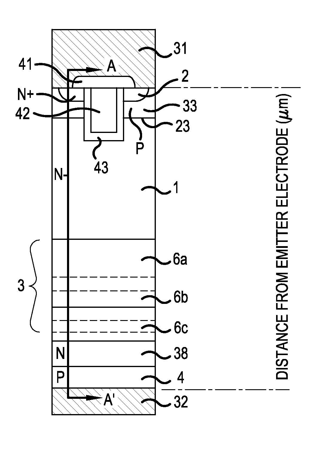
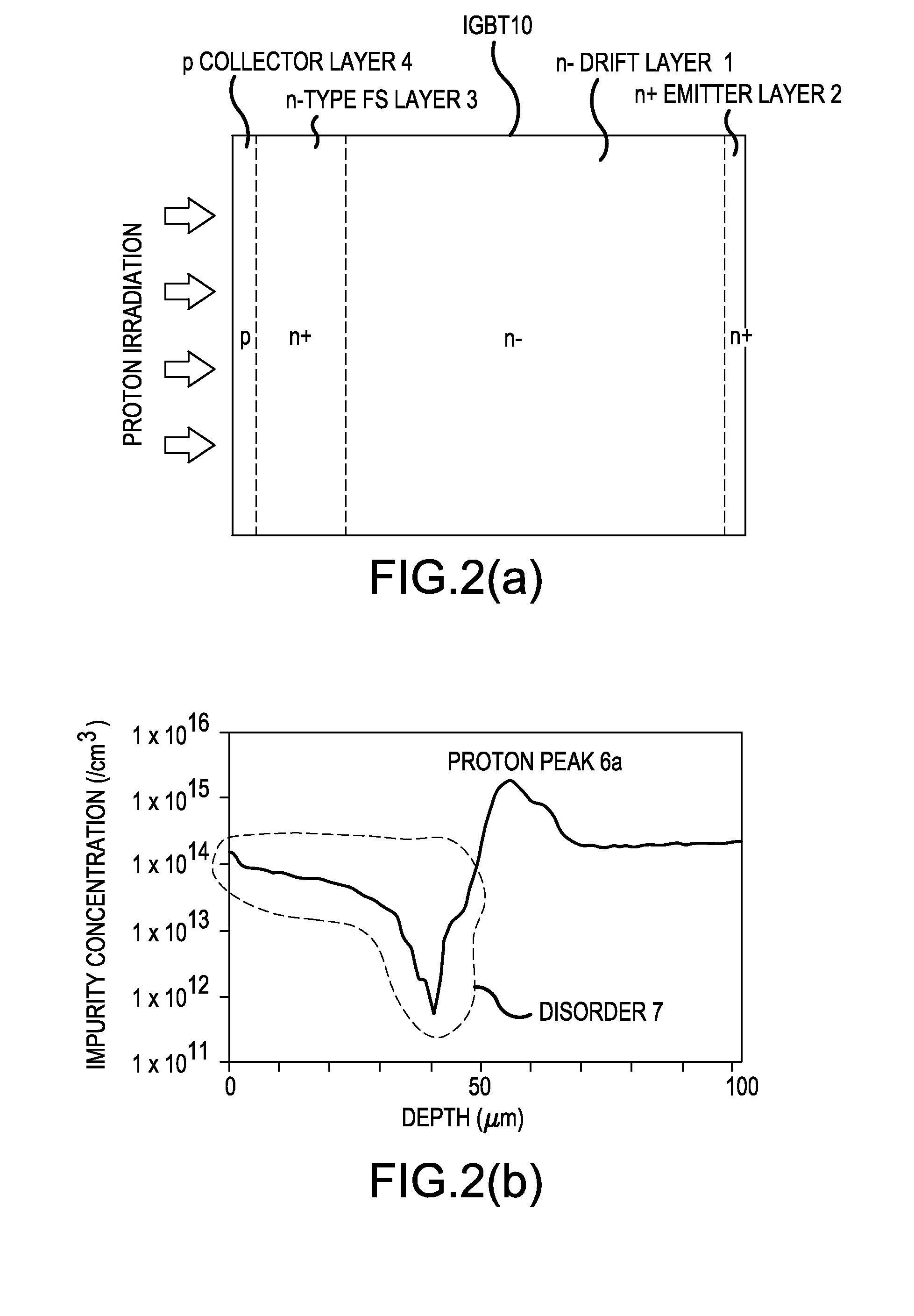
[0047]FIG. 2 is a cross-sectional view schematically illustrating the structure of a general IGBT. FIG. 2(a) is a schematic cross-sectional view illustrating the IGBT including an n-type field stop (FS) layer 3 which is formed by a general proton irradiation method according to the related art. FIG. 2(b) shows the impurity concentration profile of the n-type FS layer 3 which is measured by a known spreading resistance (SR) measurement method. However, in the schematic cross-sectional view of the IGBT, which is an example of the semiconductor device according to the invention, the semiconductor device according to the invention has the same layer structure as that shown in FIG. 2(a). Therefore, the cross-sectional view shown in FIG. 2(a) is used in the description of the semiconductor device according to the invention. An IGBT produced by a semiconductor device production method according to the invention differs from the IGBT produced by the method according to the related method in...

embodiment 2

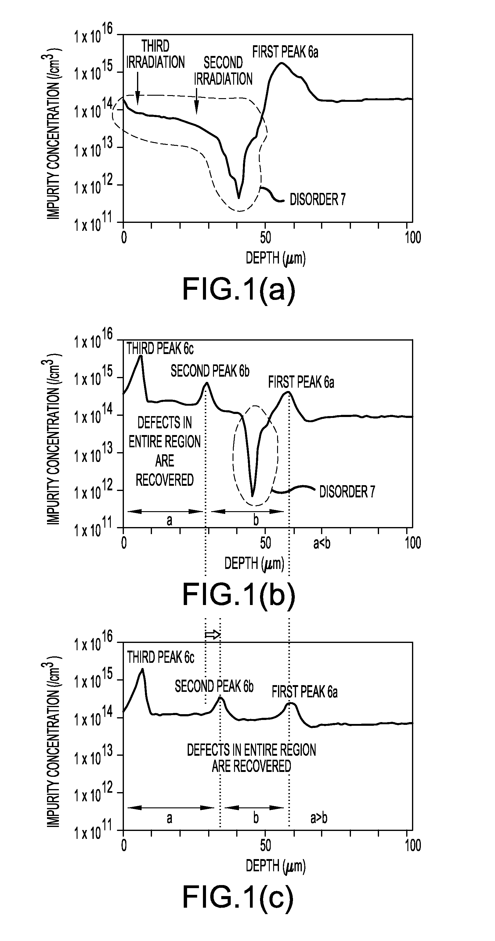
[0072]FIG. 5 is a characteristic diagram illustrating the impurity concentration profile of an n-type FS layer in a semiconductor device according to Embodiment 2. A semiconductor device production method according to Embodiment 2 differs from the semiconductor device production method according to Embodiment 1 in that a plurality of proton irradiation operations for removing disorder 17 or reducing the degree of the disorder 17 are sequentially performed from a deep position to a shallow position from the rear surface of a substrate in the region of the disorder 17.

[0073]The semiconductor device produced by the semiconductor device production method according to Embodiment 2 is, for example, an IGBT shown in FIG. 2(a), similarly to Embodiment 1. The semiconductor device production method according to Embodiment 2 is the same as the semiconductor device production method according to Embodiment 1 except for a proton irradiation method for forming an n-type FS layer 3. Therefore, onl...

embodiment 3

[0081]FIG. 6 is a characteristic diagram illustrating the impurity concentration profile of an n-type FS layer in a semiconductor device according to Embodiment 3. A semiconductor device production method according to Embodiment 3 differs from the semiconductor device production method according to Embodiment 1 in that a plurality of proton irradiation operations for removing disorder 27 or reducing the degree of the disorder 27 are sequentially performed from a shallow position to a deep position from the rear surface of a substrate in the region of the disorder 27.

[0082]A proton irradiation method according to Embodiment 3 will be described. FIGS. 6(a) to 6(c) show the impurity concentration profile of an n-type FS layer 3 after the first to third proton irradiation operations and annealing processes. As shown in FIG. 6(a), a first proton peak 26a is formed at a predetermined depth from the rear surface of the substrate by the first proton irradiation to form the region (a portion...


PUM


Abstract

Proton irradiation is performed a plurality of times from rear surface of an n-type semiconductor substrate, which is an n− drift layer, forming an n-type FS layer having lower resistance than the n-type semiconductor substrate in the rear surface of the n− drift layer. When the proton irradiation is performed a plurality of times, the next proton irradiation is performed to as to compensate for a reduction in mobility due to disorder which remains after the previous proton irradiation. In this case, the second or subsequent proton irradiation is performed at the position of the disorder which is formed by the previous proton irradiation. In this way, even after proton irradiation and a heat treatment, the disorder is reduced and it is possible to prevent deterioration of characteristics, such as increase in leakage current. It is possible to form an n-type FS layer including a high-concentration hydrogen-related donor layer.

Description

BACKGROUND OF THE INVENTION[0001]A. Field of the Invention[0002]The present invention relates to a semiconductor device and a method for producing a semiconductor device.[0003]B. Description of the Related Art[0004]A power conversion apparatus, such as a converter-inverter system essential for the control of a rotary motor or a servo-motor, has been known. In order to improve the efficiency of the power conversion apparatus and to reduce the power consumption thereof, there is a strong demand for a technique capable of reducing the loss of a semiconductor device, such as a power diode or an insulated gate bipolar transistor (IGBT) provided in the power conversion apparatus.[0005]As one of the methods for meeting the demand for the technique capable of reducing the loss, for a diode or an IGBT, a field stop (FS) layer structure has been known in which a drift layer, which is a thick layer with the highest resistance, among semiconductor layers forming an element structure is thinned ...

Claims


Application Information

Patent Timeline
Patent Type & Authority Applications(United States)
IPC IPC(8): H01L29/32H01L29/861H01L29/10H01L29/739
CPCH01L29/32H01L29/1095H01L29/861H01L29/7395H01L21/263H01L29/66348H01L29/7397H01L21/265H01L21/324H01L21/326H01L29/70H01L29/739H01L29/78H01L29/868H01L29/0615H01L29/36H01L29/6609H01L29/66333
Inventor TAKISHITA, HIROSHIYOSHIMURA, TAKASHIMIYAZAKI, MASAYUKIKURIBAYASHI, HIDENAO
Owner FUJI ELECTRIC CO LTD
Why Eureka
Try Eureka