Plug structure and process thereof

a technology of plug and socket, applied in the direction of semiconductor devices, semiconductor/solid-state device details, electrical apparatus, etc., to achieve the effect of enhancing the adhesion between the first contact plug and the second contact plug

Active Publication Date: 2014-09-18
UNITED MICROELECTRONICS CORP
View PDF5 Cites 6 Cited by
  • Summary
  • Abstract
  • Description
  • Claims
  • Application Information

AI Technical Summary

Benefits of technology

[0005]The present invention provides a plug structure and a process thereof, which performs a sputtering process to remove at least part of a bottom part of a barrier layer, to improve the performance of a formed semiconductor component.
[0008]According to the above, the present invention provides a plug structure and a process thereof, which performs a first sputtering process to remove a bottom part of at least one layer of a barrier layer, so the contact resistance (Rc) between each of a first contact plug and a second contact plug can be reduced. The adhesion between the first contact plug and the second contact plug can be enhanced, and the top critical dimension (CD) of the barrier layer and the opening filling can be improved.

Problems solved by technology

As the miniaturization of semiconductor devices increases, filling the barrier layer and the low resistivity material into a contact hole has become an important issue to form the contact plug and maintaining or enhancing the performances of formed semiconductor devices as well.

Method used


Image

  • Plug structure and process thereof
  • Plug structure and process thereof
  • Plug structure and process thereof

Examples


Embodiment Construction

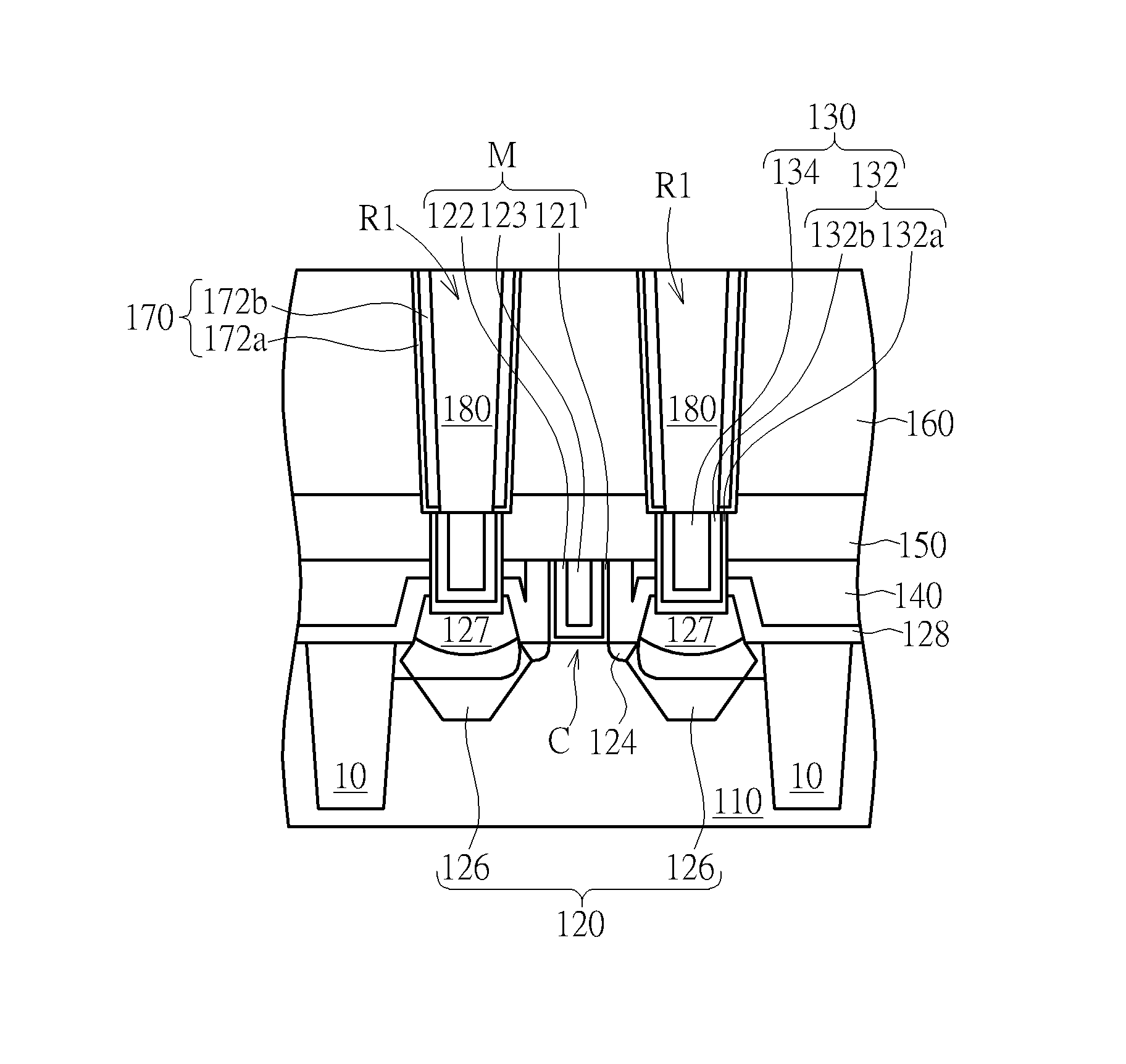
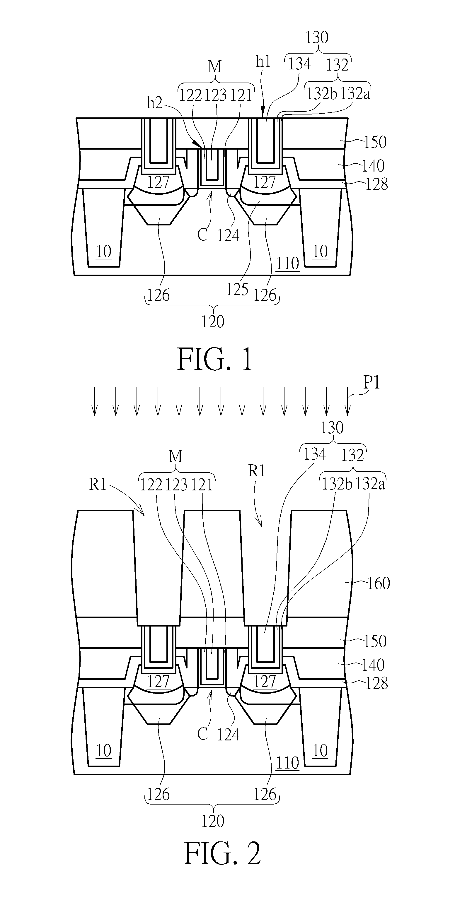
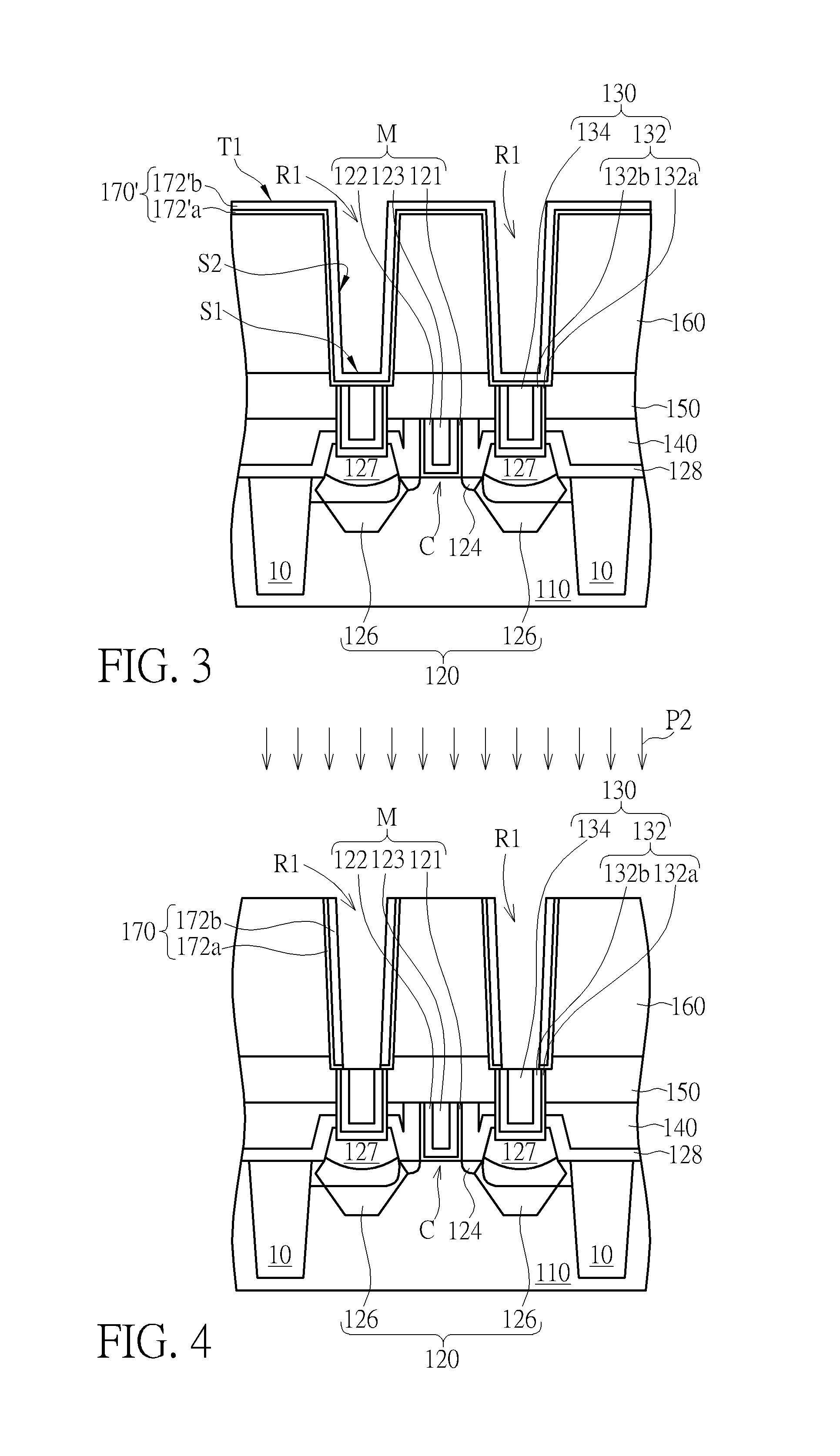
[0014]FIGS. 1-6 schematically depict cross-sectional views of a method of forming a plug structure according to a first embodiment of the present invention. As shown in FIG. 1, a substrate 110 is provided. The substrate 110 may be a semiconductor substrate such as a silicon substrate, a silicon containing substrate, a III-V group-on-silicon (such as GaN-on-silicon) substrate, a graphene-on-silicon substrate or a silicon-on-insulator (SOI) substrate. Isolation structures 10 are formed in the substrate 110 to electrically isolate each MOS transistor. A MOS transistor 120 is formed on / in the substrate 110. The MOS transistor 120 may include a metal gate M on the substrate, and the metal gate M may includes a stacked structure including a dielectric layer 121, a work function layer 122 and a low resistivity material 123 sequentially from bottom to top; a lightly doped source / drain 124, a source / drain 125 and an epitaxial structure 126 are formed in the substrate 110 beside the metal gat...


PUM


Abstract

A plug structure including a first dielectric layer, a second dielectric layer, a barrier layer and a second plug is provided. The first dielectric layer having a first plug therein is located on a substrate, wherein the first plug physically contacts a source / drain in the substrate. The second dielectric layer having an opening exposing the first plug is located on the first dielectric layer. The barrier layer conformally covers the opening, wherein the barrier layer has a bottom part and a sidewall part, and the bottom part is a single layer and physically contacts the first plug while the sidewall part is a dual layer. The second plug fills the opening and on the barrier layer. Moreover, a process of forming a plug structure is also provided.

Description

BACKGROUND OF THE INVENTION[0001]1. Field of the Invention[0002]The present invention relates generally to a plug structure and a process thereof, and more specifically to a plug structure and a process thereof that removes parts of barrier layers by performing an argon sputtering process.[0003]2. Description of the Prior Art[0004]Field effect transistors are important electronic devices in the fabrication of integrated circuits, and as the size of the semiconductor device becomes smaller and smaller, the fabrication of the transistors also improves and is constantly enhanced for fabricating transistors with smaller sizes and higher quality. In the conventional method of fabricating transistors, agate structure is first formed on a substrate, and a lightly doped drain (LDD) is formed on the two corresponding sides of the gate structure. Then, a spacer is formed on the sidewall of the gate structure and an ion implantation process is performed to form a source / drain within the substr...

Claims


Application Information

Patent Timeline
Patent Type & Authority Applications(United States)
IPC IPC(8): H01L21/768H01L23/538
CPCH01L23/5384H01L21/76841H01L23/485H01L21/76844H01L2924/0002H01L2924/00
Inventor HUNG, CHING-WENHUANG, CHIH-SENTSAO, PO-CHAO
Owner UNITED MICROELECTRONICS CORP
Why Eureka
Try Eureka